Publication number: 20200127357
Type: Application
Filed: Apr 27, 2018
Publication Date: Apr 23, 2020
Patent Grant number: 11394097
Inventors: Senad Bulja (Dublin), Rose Fasano Kopf (Green Brook, NJ), Pawel Rulikowski (Clonsilla), Majid Norooziarab (Dublin)
Application Number: 16/611,056
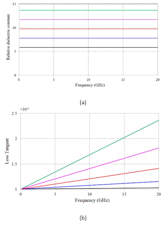
Abstract: In this invention a new type of multilayered RF substrates is proposed, capable of achieving an arbitrary dielectric characteristic. Such a substrate is illustrated in Fig.1 and consists of several layers of interlaced dielectric and sub-skin depth conductor thicknesses. The invention makes use of the fact that at sub-skin depths, conductors effectively behave as high dielectric constant dielectrics. Interlacing such conductors with dielectrics allows one to achieve an almost arbitrary dielectric characteristic of the entire dielectric stack, as a function of conductor thickness. An example of achievable dielectric characteristics is shown in Fig. 2, when the dielectric is silicon dioxide (SiO2) with a thickness of 10 nm and conductor is copper with thickness varied from 10 nm to 50 nm in increments of 10 nm.


The dielectric material is silicon dioxide (r=3.9) and the conductor layer is copper. The thicknesses of copper layers are 10 nm (black), 20 nm (blue), 30 nm (red), 40 nm (magenta) and 50 nm (green)
As evident, the dielectric characteristic permittivity changes from nominal r=3.9 (no conductor interlacing) to r=13 with 50 nm copper interlacing, with a small change in dielectric loss.


Leave a Reply