Dr. Senad Bulja, PhD, FIET, SMIEEE

  • Home
  • Researches
  • Workshops
  • Patents
  • Products
  • Tutorials
  • Solutions
  • Services

Patents

Home » Patents » Structure and method of manufacturing a structure for guiding electromagnetic waves

Structure and method of manufacturing a structure for guiding electromagnetic waves

Dr. Senad Bulja 15/03/2023Download Here

Publication number: 20200411942
Type: Application
Filed: Jun 26, 2020
Publication Date: Dec 31, 2020
Applicant: Nokia Solutions and Networks Oy (Espoo)
Inventors: Florian Pivit (Dublin), Senad Bulja (Dublin)
Application Number: 16/913,790

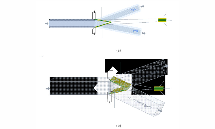
Abstract: In this invention submission a method for direct integration of PCB structures with 3D printed parts. The method is exemplarily illustrated with reference to Figure 1.

Figure 1: PCB-waveguide transitions

Chia sẻ0
Tweet
Chia sẻ

Leave a Reply Cancel reply

Your email address will not be published. Required fields are marked *

Other Posts

Figure 1 Exemplarily embodiments of PMF based RF splitting/switching device, enabled by TMO or EC material (a) and Exemplarily embodiment of air cavity waveguide-based RF splitting/switching device, enabled by TMO or EC material (b)

Controllable radio frequency switching and/or splitting device

equivalent circuit for implicit coupling among replicated resonators

Radio communications

Figure 1: All exemplary Wi-Fi operation states

Filtration for radio access technologies

Profile & Bio

Senad Bulja, Ph.D., FIET, SMIEEE 

  1. Dr Bulja’s profile
  2. Email : contact@drbulja.com

PROFESSIONAL Profile

  • Accomplished career of over 19 years demonstrating consistent success as a Researcher, Leader and Mentor in the Wireless industry research environment.
  • Excellent Scientific contributions in the field of RF, EMC and telecommunications with 4 Nature Journal publications and over 70 peer-reviewed articles and conference papers
  • Strong leadership skills demonstrated by leading Ph.D. level educated cross-continental and cross-departmental teams to successful project execution.  
  • Proven Strategic Business Impact – introduced own developed technology into Nokia’s future technology roadmap (RF filters) and business transfer of the smart surface technology. 
  • Creative, internationally awarded and well-driven inventor with over 70 filed patents in the area of hardware for Radio Frequency (RF), Wireless Sensor Networks (WSN), Internet of Things (IoT) and wireless systems architectures. E.g. Nokia patent award entitled: “A top inventor in implementation patent first filings”, 2020.
  • Significant contribution in the identification of high revenue IP assets and leadership on the creation of Nokia’s patent portfolio roadmap. 
 

© Copyright 2023 drbulja.com. All Rights reserved