Dr. Senad Bulja, PhD, FIET, SMIEEE

  • Home
  • Researches
  • Workshops
  • Patents
  • Products
  • Tutorials
  • Solutions
  • Services

Patents

Home » Patents » Electrochromic cell

Electrochromic cell

Dr. Senad Bulja 13/03/2023Download Here

Publication number: 20190346730
Type: Application
Filed: May 14, 2018
Publication Date: Nov 14, 2019
Patent Grant number: 10732476
Inventors: Senad BULJA (Dublin), Rose KOPF (Greenbrook, NJ), Florian PIVIT (Lucan), Wolfgang TEMPL (Sersheim)
Application Number: 15/978,370

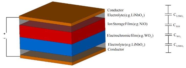
In this invention a new structure of EC cell is disclosed. A basic structure of an EC cell is shown in Fig. 1 (a). The ability to tune the high frequency dielectric and optical properties using the standard EC cell was first demonstrated in [1], while in [2] it was shown that the absolute values and the degree of dielectric and optical tunability can be varied in a simple manner – by modifying the heights of substrate layers. The extent of tunability reported was of the order of 20%. The new cell of Fig. 2 features the Ion Storage Film and Electrochromic film moved away from the contact electrodes into the interior of the EC cell. The main reason for this is to avoid shortening the channel height due to the dielectric to metal transition of transition metal oxide layers (Ion Storage and Electrochromic) upon Li ions injection as done with a standard EC cell. The electrolyte layer, on the other hand, was split into two layers and positioned at the point of contact with the bottom and top electrodes. The main reason for this lies with the fact the electrolyte does not exhibit a dielectric to metal transition by losing ions and, therefore, can be positioned in direct contact with top and bottom electrodes. Such an arrangement allows for a greater degree of dielectric tunability and lower dielectric losses, since the channel height is not shortened.  The dielectric tunability achieved with the new structure of the EC cell is no less than 60%, which is over 3 times greater than is the case with the standard EC cell.    

5gFigure 1 Basic structure of standard inorganic EC cell: perspective view (left) and capacitance model (right).

Figure 2 Basic structure of new, proposed EC cell: perspective view (left) and capacitance model (right)

[1] Bulja, S. et al. High Frequency Dielectric Characteristics of Electrochromic, WO3 and NiO Films with LiNbO3 Electrolyte. Sci. Rep. 6, 28839; doi: 10.1038/srep28839 (2016).

Chia sẻ0
Tweet
Chia sẻ

Leave a Reply Cancel reply

Your email address will not be published. Required fields are marked *

Other Posts

Figure 1 Exemplarily embodiments of PMF based RF splitting/switching device, enabled by TMO or EC material (a) and Exemplarily embodiment of air cavity waveguide-based RF splitting/switching device, enabled by TMO or EC material (b)

Controllable radio frequency switching and/or splitting device

equivalent circuit for implicit coupling among replicated resonators

Radio communications

Figure 1: All exemplary Wi-Fi operation states

Filtration for radio access technologies

Profile & Bio

Senad Bulja, Ph.D., FIET, SMIEEE 

  1. Dr Bulja’s profile
  2. Email : contact@drbulja.com

PROFESSIONAL Profile

  • Accomplished career of over 19 years demonstrating consistent success as a Researcher, Leader and Mentor in the Wireless industry research environment.
  • Excellent Scientific contributions in the field of RF, EMC and telecommunications with 4 Nature Journal publications and over 70 peer-reviewed articles and conference papers
  • Strong leadership skills demonstrated by leading Ph.D. level educated cross-continental and cross-departmental teams to successful project execution.  
  • Proven Strategic Business Impact – introduced own developed technology into Nokia’s future technology roadmap (RF filters) and business transfer of the smart surface technology. 
  • Creative, internationally awarded and well-driven inventor with over 70 filed patents in the area of hardware for Radio Frequency (RF), Wireless Sensor Networks (WSN), Internet of Things (IoT) and wireless systems architectures. E.g. Nokia patent award entitled: “A top inventor in implementation patent first filings”, 2020.
  • Significant contribution in the identification of high revenue IP assets and leadership on the creation of Nokia’s patent portfolio roadmap. 
 

© Copyright 2023 drbulja.com. All Rights reserved