
Summary
A continuously variable power divider was designed, simulated, fabricated and tested for its performance against the specifications. The power divider is made to operate at a centre frequency of 10 GHz and exhibits a power division ratio of over 30 dB and is controllable using a variable dc power supply with a dc bias voltage ranging from 0V to 15V. Details of the design, together with the summary of its performance are given in the next sections.
Design
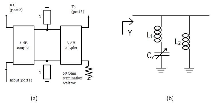
The design of the power divider is based on the circuit shown in Fig. 1. In its simplified form the circuit consists of 2 3-dB couplers connected back-to-back with a variable admittance circuit represented by admittance Y connected in shunt. The variable admittance circuit is crucial for the correct performance of the power divider and, in order to provide an arbitrary power division, its admittance must be able to vary from 0 to , upon an external stimulus. The circuit realization of the admittance used in the present design is shown in Fig. 1 (b). It consists of a variable capacitor diode (varactor) and two passive components (inductors). Upon variation of dc bias voltage, the reactance of the diode varies from a very low value (close to zero Ω) to a very high value (several kΩ), necessary to channel RF power between ports 2 and 3.
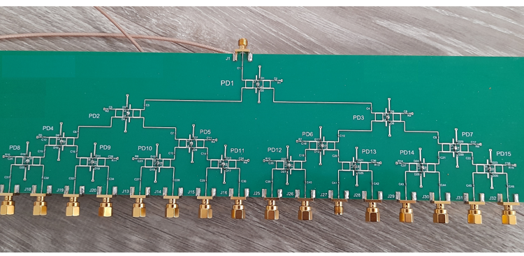
Fabricated power divider
The fabricated power divider is shown in Fig. 2. Fabrication was carried out on a FR-408 substrate with the following properties: and tan(δ) = 0.0125 at 10 GHz. The thickness of the substrate upon which the circuitry is placed is 0.2 mm (8 mil), however for rigidity, it is mounted on a thicker FR408 substrate. The height of the entire stack now stands at 0.9144 mm (36 mil). The details of the PCB stack-up are provided in the manufacturing document sent separately.
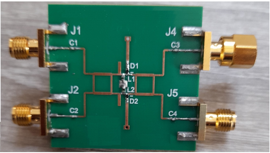
As can be seen from this figure, the individual couplers are realized as branch-line couplers with a centre frequency of operation of 10 GHz. The inductors necessary for the correct operation of shunt admittance Y are realized in the distributed form in order to reduce the insertion losses. The RF choke is 0402 inductor with a nominal inductance of 3.2 nH, however, its inductance at 10 GHz is much higher and fully prevents RF signal leakage. The DC block capacitors are also 0402 components with a stated capacitance of 0.7 pF. However, just like in the case of the RF chokes, their capacitance at 10 GHz is extremely high and effectively forms a short circuit. The variable capacitance diode is from Skyworks, with a part number SMV1231 and a package SOD882.
Results
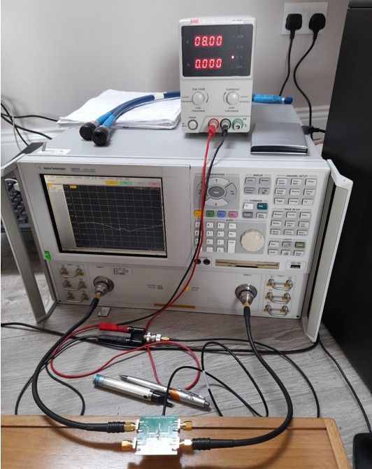
The set-up used in the measurements of the linear parameters of the power divider is shown Fig. 3.
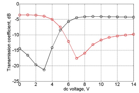
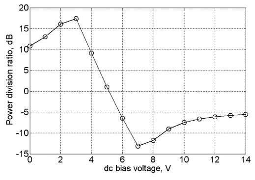
Measurements of the S-parameters are performed in the frequency window of 9 GHz to 11 GHz and for dc bias voltages 0 to 14 V (please note that the maximum dc bias voltage for the varactor diode is 15 V). Fig. 4 shows the measured S21 (from J1 to J2, Fig. 2 (a)) and S31 (from J1 to J5, Fig. 2 (a)) parameters as a function of dc bias voltage at 10 GHz, while the power division ratio, defined as the difference between S21 and S31 is shown in Fig. 5. As can be seen from this figure the power division ratio is slightly over 30 dB. The insertion losses stand at approximately 3.9 dB for S21 and 4.2 dB for S31 at 10 GHz.
The broadband (9 GHz-11 GHz) transmission and reflection coefficients are presented in Figs. 6 for several representative dc bias voltages, 3V, 7V and 14V.
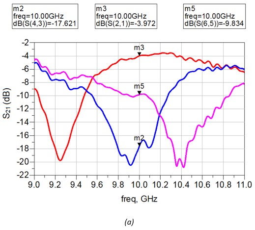
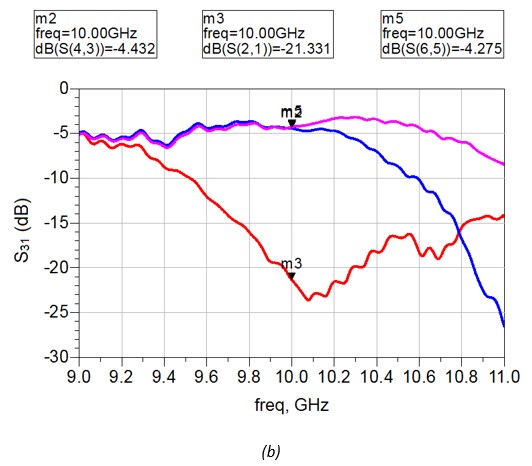
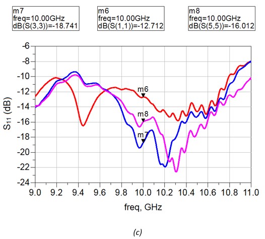
Fig. 6 Broadband S-parameters of the power divider of Fig. 2 for 3V (red), 7 V (blue) and 14 V (pink). (a) – S21, (b) – S31
The reflection coefficient is never less than 12 dB, indicating that the reflective loads are well balanced.
Conclusion and summary
A 10 GHz power divider having a 30 dB power division ratio has been designed, fabricated and tested. The measured results indicate that the variable power divider can be made on a cost-effective substrate (FR408, Isola) using cost effective elements (varactor diodes and surface mount lumped elements) and perform extremely well.
Leave a Reply