
Summary
A continuously variable single input with 16 outputs (1:16) power divider has been designed, simulated, fabricated and tested for its performance. The power divider consists of 4 attenuation stages, is made to operate at a centre frequency of 10 GHz and, according to the simulations, exhibits a power division ratio of over 80 dB. The division ratio is controlled using a variable dc power supply with a dc bias voltage ranging from 0V to 15V. Details of the design, together with the summary of its performance are given in the next sections.
Design
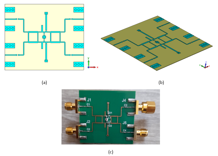
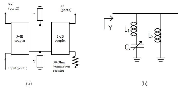
The design of the power divider is based on the circuit shown in Fig. 1. In its simplified form the circuit consists of 2 3-dB couplers connected back-to-back with a variable admittance circuit represented by admittance Y connected in shunt. The variable admittance circuit is crucial for the correct performance of the power divider and, in order to provide an arbitrary power division, its admittance must be able to vary from 0 to , upon an external stimulus. The circuit realization of the admittance used in the present design is shown in Fig. 1 (b). It consists of a variable capacitor diode (varactor) and two passive components (inductors). Upon variation of dc bias voltage, the reactance of the diode varies from a very low value (close to zero Ω) to a very high value (several kΩ), necessary to channel RF power between ports 2 and 3. This divider is referred to as “one input two outputs” (1:2) variable power divider.
 and realization of variable admittance (b)")
The designed, simulated and fabricated 1 to 2 variable power divider is shown in Fig.2.
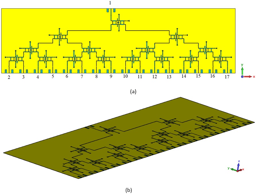
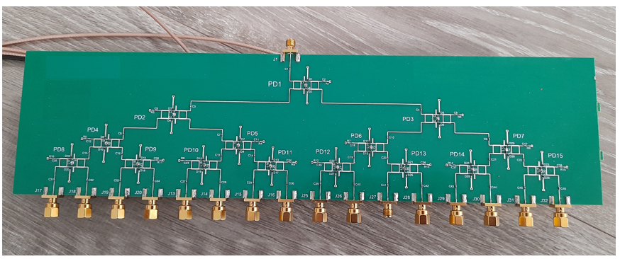
The 1:16 power divider is created by using the 1:2 variable power divider of Fig. 2 as the basis. The designed 1 to 16 variable power divider is shown in Fig. 3.
The simulated response of the variable power divider is presented in tables below for each signal path. The results pertain to the frequency of operation of 10 GHz.
Table 1 – S21 – total dynamic range: 87.512 dB. 21.87 dB per stage.
| Voltage (V) | Dynamic range (dB) | Max. power = -10.51 dB | ||
| PD1 | -73.386 to -98.022 | V1 = 15 V | 24.636 | V1 = 1.8 V |
| PD2 | -52.401 to -73.386 | V2 = 3.3 V | 20.985 | V2 = 15 V |
| PD4 | -31.445 to -52.401 | V4 = 3.3 V | 20.956 | V4 = 15 V |
| PD8 | -10.51 to -31.445 | V8 = 3.3 | 20.935 | V8 = 15 V |
Table 2 – S31 – total dynamic range: 91.333 dB. 22.83 dB per stage.
| Voltage (V) | Dynamic range (dB) | Max. power = -10.14 dB | ||
| PD1 | -76.837 to -101.473 | V1 = 15 V | 24.636 | V1 = 1.8 V |
| PD2 | -55.853 to -76.837 | V2 = 3.3 V | 20.984 | V2 = 15 V |
| PD4 | -34.764 to -55.853 | V4 = 3.3 V | 21.089 | V4 = 15 V |
| PD8 | -10.14 to -34.904 | V8 = 15 V | 27.764 | V8 = 1.8 V |
Table 3 – S41 – total dynamic range: 95.226 dB. 23.806 dB per stage.
| Voltage (V) | Dynamic range (dB) | Max. power = -9.799 dB | ||
| PD1 | -80.388 to -105.025 | V1 = 15 V | 24.637 | V1 = 1.8 V |
| PD2 | -59.37 to -80.388 | V2 = 3.3 V | 21.03 | V2 = 15 V |
| PD4 | -34.544 to -59.37 | V4 = 15 V | 24.826 | V4 = 1.7 V |
| PD9 | -9.799 to -34.544 | V9 = 15 V | 24.745 | V9 = 1.8 V |
Table 4 – S51 – total dynamic range: 91.288 dB. 22.822 dB per stage.
| Voltage (V) | Dynamic range (dB) | Max. power = -10.159 dB | ||
| PD1 | -76.974 to -101.447 | V1 = 15 V | 24.473 | V1 = 1.8 V |
| PD2 | -55.944 to -76.974 | V2 = 3.3 V | 21.03 | V2 = 15 V |
| PD4 | -31.103 to -55.944 | V4 = 15 V | 24.841 | V4 = 1.7 V |
| PD9 | -10.159 to -31.103 | V9 = 3.3 V | 20.944 | V9 = 15 V |
Table 5 – S61 – total dynamic range: 94.63 dB. 23.65 dB per stage.
| Voltage (V) | Dynamic range (dB) | Max. power = -9.874 dB | ||
| PD1 | -80.105 to -104.504 | V1 = 15 V | 24.399 | V1 = 1.7 V |
| PD2 | -55.521 to -80.105 | V2 = 15 V | 24.584 | V2 = 1.8 V |
| PD5 | -30.835 to -55.521 | V5 = 15 V | 24.686 | V5 = 1.7 V |
| PD10 | -9.874 to -30.835 | V10 = 3.3 V | 20.961 | V10 = 15 V |
Table 6 – S71 – total dynamic range: 98.402 dB. 24.6005 dB per stage.
| Voltage (V) | Dynamic range (dB) | Max. power = -9.874 dB | ||
| PD1 | -83.531 to -107.93 | V1 = 15 V | 24.399 | V1 = 1.8 V |
| PD2 | -58.947 to -83.531 | V2 = 15 V | 24.584 | V2 = 1.8 V |
| PD5 | -34.259 to -58.947 | V5 = 15 V | 24.688 | V5 = 1.7 V |
| PD10 | -9.528 to -34.259 | V10 = 15 V | 24.731 | V10 = 1.8 V |
Table 7 – S81 – total dynamic range: 94.682 dB. 23.6705 dB per stage.
| Voltage (V) | Dynamic range (dB) | Max. power = -9.826 dB | ||
| PD1 | -80.109 to -104.508 | V1 = 15 V | 24.399 | V1 = 1.8 V |
| PD2 | -55.546 to -80.109 | V2 = 15 V | 24.563 | V2 = 1.8 V |
| PD5 | -34.58 to -55.546 | V5 = 3.3 V | 20.966 | V5 = 15 V |
| PD11 | -9.826 to -34.58 | V11 = 15 V | 24.754 | V11 = 1.8 V |
Table 8 – S91 – total dynamic range: 90.862 dB. 22.7155 dB per stage.
| Voltage (V) | Dynamic range (dB) | Max. power = -10.195 dB | ||
| PD1 | -76.658 to -101.057 | V1 = 15 V | 24.399 | V1 = 1.8 V |
| PD2 | -52.095 to -76.658 | V2 = 15 V | 24.563 | V2 = 1.8 V |
| PD5 | -31.132 to -52.095 | V5 = 3.3 V | 20.963 | V5 = 15 V |
| PD11 | -10.195 to -31.132 | V11 = 3.3 V | 20.937 | V11 = 15 V |
Table 9 – S10,1 – total dynamic range: 87.45 dB. 21.86 dB per stage.
| Voltage (V) | Dynamic range (dB) | Max. power = -10.549 dB | ||
| PD1 | -77.033 to -97.999 | V1 = 3.3 V | 20.966 | V1 = 15 V |
| PD3 | -52.47 to -77.033 | V3 = 15 V | 24.563 | V3 = 1.8 V |
| PD6 | -31.484 to -52.47 | V6 = 3.3 V | 20.986 | V6 = 15 V |
| PD12 | -10.549 to -31.484 | V12 = 3.3 V | 20.935 | V12 = 15 V |
Table 10 – S11,1 – total dynamic range: 91.271 dB. 22.81 dB per stage.
| Voltage (V) | Dynamic range (dB) | Max. power = -10.179 dB | ||
| PD1 | -80.484 to -101.45 | V1 = 3.3 V | 20.966 | V1 = 15 V |
| PD3 | -55.921 to -80.484 | V3 = 15 V | 24.563 | V3 = 1.8 V |
| PD6 | -34.934 to -55.921 | V6 = 3.3 V | 20.987 | V6 = 15 V |
| PD12 | -10.179 to -34.934 | V12 = 15 V | 24.755 | V12 = 1.8 V |
Table 11 – S12,1 – total dynamic range: 95.12 dB. 23.78 dB per stage.
| Voltage (V) | Dynamic range (dB) | Max. power = -9.876 dB | ||
| PD1 | -83.987 to -104.996 | V1 = 3.3 V | 20.966 | V1 = 15 V |
| PD3 | -59.4 to -83.987 | V3 = 15 V | 24.563 | V3 = 1.7 V |
| PD6 | -34.608 to -59.4 | V6 =15 V | 24.792 | V6 = 1.8 V |
| PD13 | -9.876 to -34.608 | V13 = 15 V | 24.731 | V13 = 1.8 V |
Table 12 – S13,1 – total dynamic range: 91.348 dB. 22.837 dB per stage.
| Voltage (V) | Dynamic range (dB) | Max. power = -10.222 dB | ||
| PD1 | -80.561 to -101.57 | V1 = 3.3 V | 21.009 | V1 = 15 V |
| PD3 | -55.974 to -80.561 | V3 = 15 V | 24.587 | V3 = 1.7 V |
| PD6 | -31.182 to -55.974 | V6 =15 V | 24.792 | V6 = 1.8 V |
| PD13 | -10.222 to -31.182 | V13 = 3.3 V | 20.96 | V13 = 15 V |
Table 13 – S14,1 – total dynamic range: 87.673 dB. 21.91 dB per stage.
| Voltage (V) | Dynamic range (dB) | Max. power = -10.506 dB | ||
| PD1 | -77.153 to -98.179 | V1 = 3.3 V | 21.026 | V1 = 15 V |
| PD3 | -56.178 to -77.153 | V3 = 3.3 V | 24.587 | V3 = 15 V |
| PD7 | -31.448 to -56.178 | V7 =15 V | 24.73 | V7 = 1.7 V |
| PD14 | -10.506 to -31.448 | V14 = 3.3 V | 20.942 | V14 = 15 V |
Table 14 – S15,1 – total dynamic range: 91.461 dB. 22.86 dB per stage.
| Voltage (V) | Dynamic range (dB) | Max. power = -10.145 dB | ||
| PD1 | -80.579 to -101.606 | V1 = 3.3 V | 21.027 | V1 = 15 V |
| PD3 | -59.605 to -80.579 | V3 = 3.3 V | 20.974 | V3 = 15 V |
| PD7 | -34.892 to -59.605 | V7 =15 V | 24.73 | V7 = 1.7 V |
| PD14 | -10.145 to -34.892 | V14 = 15 V | 24.747 | V14 = 1.7 V |
Table 15 – S16,1 – total dynamic range: 87.661 dB. 21.91 dB per stage.
| Voltage (V) | Dynamic range (dB) | Max. power = -10.495 dB | ||
| PD1 | -77.129 to -98.156 | V1 = 3.3 V | 21.027 | V1 = 15 V |
| PD3 | -56.17 to -77.129 | V3 = 3.3 V | 20.959 | V3 = 15 V |
| PD7 | -35.254 to -56.17 | V7 =3.3 V | 20.916 | V7 = 15 V |
| PD15 | -10.495 to -35.254 | V15 = 15 V | 24.759 | V15 = 1.7 V |
Table 16 – S17,1 – total dynamic range: 83.836 dB. 20.959 dB per stage.
| Voltage (V) | Dynamic range (dB) | Max. power = -10.869 dB | ||
| PD1 | -73.678 to -94.705 | V1 = 3.3 V | 21.027 | V1 = 15 V |
| PD3 | -52.719 to -73.678 | V3 = 3.3 V | 20.959 | V3 = 15 V |
| PD7 | -31.796 to -52.719 | V7 =3.3 V | 20.923 | V7 = 15 V |
| PD15 | -10.869 to -31.796 | V15 = 3.3 V | 20.927 | V15 = 15 V |
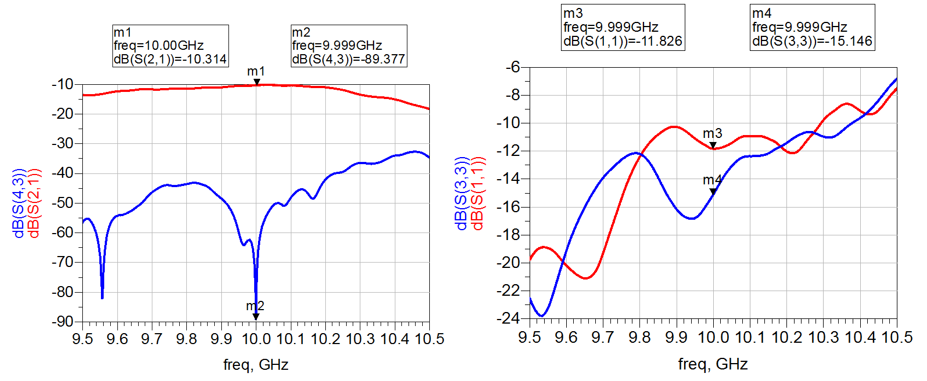
The simulated S-parameters for ports 1 and 2 over a frequency range between 9.5 GHz to 10.5 GHz are presented in Figs.
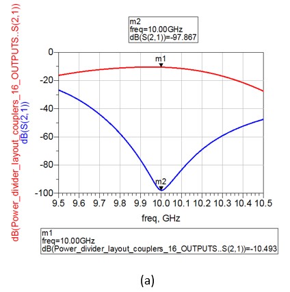
Fig. 4 Simulated S-parameters for ports 1 and 2; (a) – transmission coefficient and (b) reflection coefficient. Blue – fully OFF state and Red – fully ON state
The red curve in this figure refers to the case when all input power redirected to port 2, while the blue curve refers to the case when no power is directed toward port 3. As can be seen from this figure, the dynamic range is well over 80 dB at a frequency of 10 GHz.
Fabricated power divider
The fabricated 1 to 16 variable power divider is shown in Fig. 5. Fabrication was carried out on a FR-408 substrate with the following properties: and tan(δ) = 0.0125 at 10 GHz. The thickness of the substrate upon which the circuitry is placed is 0.2 mm (8 mil), however for rigidity, it is mounted on a thicker FR408 substrate. The height of the entire stack now stands at 0.9144 mm (36 mil).
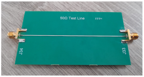
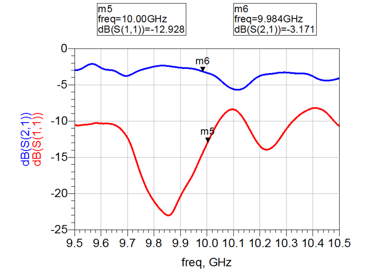
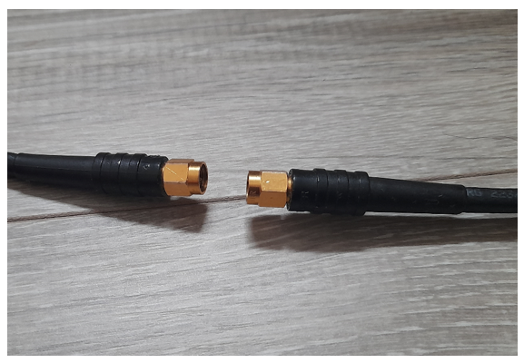
Prior to the measurements of the entire active board, it is imperative to check the performance of the through line, in order to ensure that the return losses are in line with the simulations. This will give one an indication on the accuracy of the fabrication. The fabricated 50 Ω line is shown in Fig. 6. The measured S-parameters of the line are shown in Fig. 7. As can be seen from this figure, the line is reasonably-well matched with a return loss lower than -12 dB at a frequency of 10 GHz. The insertion loss at the same frequency stands at approximately 3 dB, which is reasonable.
The single-frequency (10 GHz) measured performance of the 1 to 16 variable power divider for ports 1, 2, and 12 is presented in Tables 17-18. As can be seen from these tables, the dynamic range for S21 is around 80 dB, while
Table 17 – S21 – total dynamic range: 79.02 dB. 19.75 dB per stage.
| Voltage (V) | Dynamic range (dB) | Max. power = -10.35 dB | ||
| PD1 | -89.37 dB | V1 = 4.61 V | 24.636 | V1 = 0.64 V |
| PD2 | V2 = 1.5 V | V2 = 14.56 V | ||
| PD4 | V4 = 3.15 V | V4 = 14.53 V | ||
| PD8 | -10.35 dB | V8 = 0 V | V8 = 14.59 V | |
| PD3 | V3 = 5.55 |
Table 18 – S12,1 – total dynamic range: 56.11 dB. 14 dB per stage.
| Voltage (V) | Dynamic range (dB) | Max. power = -14.1 dB | ||
| PD1 | -70.21 | V1 = 5.06 V | 20.966 | V1 = 14.85 V |
| PD3 | V3 = 4.42 V | 24.563 | V3 = 0 V | |
| PD6 | V6 =5.88 V | 24.792 | V6 = 0 V | |
| PD13 | -14.1 | V13 = 6.39 V | 24.731 | V13 = 0 V |
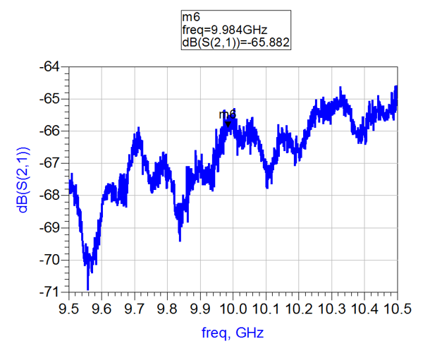
the dynamic range for the S21,1 path is around 56 dB, both somewhat lower compared to the ones predicted by simulations. There are two reasons for this behavior. First, there always exist unaccounted for losses in the circuit which prevent the exact match between the measurements and simulations. This is usually made worse when the Device-Under-Test (DUT) is resonant, as is the case here. Second, in the fully OFF state the signal is attenuated to the very low level (between -90 dB and -80 dB) which can create problems for the internal receiver inside the Vector Network Analyser (VNA) to accurately measure the signal. In other words, the received signal is almost indistinguishable from noise. To illustrate this point, Fig. 8 shows the transmission coefficient for the case when no DUT is connected and the VNA cables are separated by approximately 1.5 cm, as shown in Fig. 9. As can be seen, the transmission coefficient is very low, almost buried in noise.
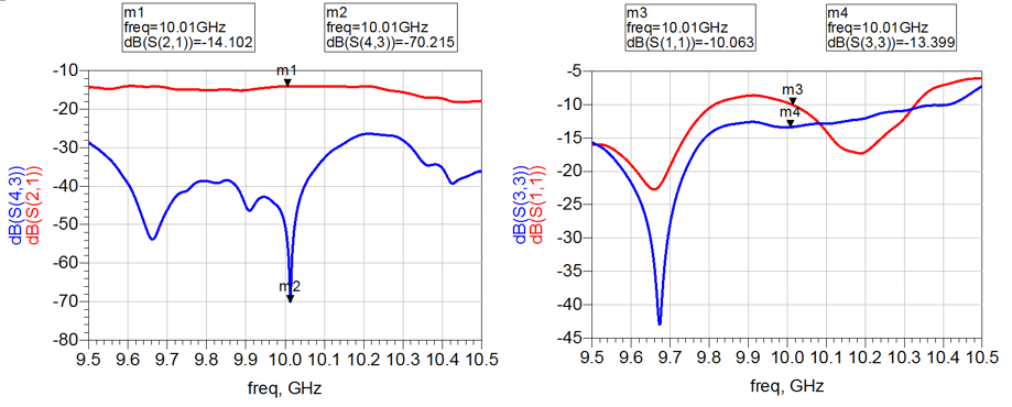
The measured S-parameters for ports 1, 2 and 12 over a frequency range between 9.5 GHz to 10.5 GHz are presented in Figs. 10 and 11. As can be seen from these figures, the insertion loss in a fully on state varies from -10.2 dB (port 2) and 14.15 dB (port 12). The insertion loss at port 2 is fully in line with the simulations, however, the measured insertion loss at port 12 is lower than predicted by approximately 3.5 dB. There are several possible reasons for this behaviour:
- There exist unaccounted for losses in the measurements. These are usually difficult to predict and analyse, since their source may lie with low-level manufacturing imperfections.
- The return losses are not as low as predicted by simulations, which adversely affects the insertion losses. Higher return losses in 3-dB coupler structures occur only when its loads are not balanced, pointing to possible assembly issues. Due to the fact that the board was manually assembled, there exist a possibility that an uneven amount of solder was used for the reflective loads of the couplers. However, this can be ameliorated during the next stage through the use of automatic assembly processes.
Lastly, it will be instructive to gauge the performance of the individual power dividers. This is done for the S21 transmission coefficient (J1 – J17, Fig. 5) in a systematic manner. First, the dc bias voltages are set for the case when the transmission coefficient is at a maximum. This case corresponds Fig. 10. Then, in order to avoid the possibility of attenuating the signal to the level that is indistinguishable from the noise, the dc bias voltage on only one power divider at a time is changed and the dynamic range is measured. Mathematically, this can be expressed:
, where i = 1,2,4,8 (1)
In this way, the dynamic range of each power divider can be assessed without an uncertainty of the signal level being too low for the receiver. The achieved dynamic ranges of each power divider are shown in Table 19.
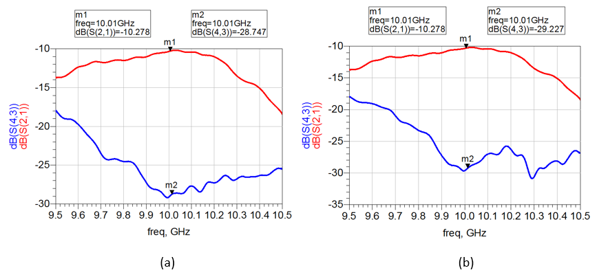
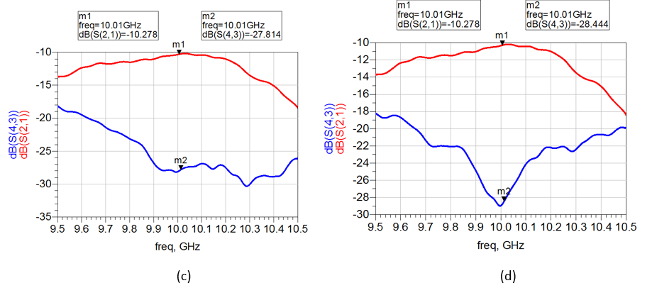
Table 19 – Measured dynamic range of each stage for the transmission coefficient (J1-J17), enabled by power dividers PD1, PD2, PD4 and PD8.
| S21 max (dB) | S21 max with PDs OFF (dB) | Dynamic range (dB) | Average dynamic range (dB) | |
| PD1 | -10.27 | -28.74 | 18.47 | 18.27 |
| PD2 | -10.27 | -29.2 | 18.93 | 18.27 |
| PD4 | -10.27 | -27.81 | 17.54 | 18.27 |
| PD8 | -10.27 | -28.44 | 18.17 | 18.27 |
The measured dynamic range is very close to the one predicted by the simulations – 18.27 dB vs 21.87 dB (same paths, J1-J17), which is an indication that the fabricated variable power splitter performs pretty much in line with the predictions. The difference in the dynamic range of about 3.6 dB is relatively small given the attenuation range and could well be attributed to imperfect manufacturing, unbalanced varactor diodes and possible assembly errors. The assembly errors are likely to stem from the fact that the individual components are manually soldered, inferring that small soldering imperfections are unavoidable.
When all aspects are considered, it is believed than the fabricated 1 to 16 variable power divider performs very well. The power divider still exhibits dynamic ranges between 56 and 80 dB, which is excellent for many applications.
Conclusion and summary
A four-stage, 1 to 16, 10 GHz variable power divider having a designed power division ratio around 90 has been designed, fabricated and tested. The measurements indicate a power division ratio between 56 dB and 80 dB, which, even though lower than predicted by simulations, is very reasonable. The measured return losses, however, are somewhat lower than predicted by simulations – on average the simulated return losses are -20 dB, whereas the measured return losses vary between -10 dB and -15 dB, depending on the biasing conditions. Since low return losses are primarily due to imbalanced reflective loads, it is believed that this could be due to uncertainties incurred during manual assembly of the PCB and associated components, in particular soldering of the very small components. It is believed that this could be addressed at the next stage of the power divider development, through the use of an automatic assembly process.
Leave a Reply