Dr. Senad Bulja, PhD, FIET, SMIEEE

  • Home
  • Researches
  • Workshops
  • Patents
  • Products
  • Tutorials
  • Solutions
  • Services

Researches

Home » Researches » Variable Temperature Broadband Microwave and Millimeter-Wave Characterization of Electrochromic (WO3/LiNbO3/NiO) Thin Films

Variable Temperature Broadband Microwave and Millimeter-Wave Characterization of Electrochromic (WO3/LiNbO3/NiO) Thin Films

Dr. Senad Bulja 04/01/2023Download Here


In our previous papers on Electro-Chromic (EC) materials, we have shown that standard inorganic EC structures in the form of EC film/electrolyte/Ion storage films (such as WO3/LiNbO3/NiO) and advanced structures in the form of electrolyte/EC film/Ion storage/ electrolyte, such as LiNbO3/WO3/NiO/LiNbO3 films in addition to possessing reconfigurable optical properties also exhibit a degree of electric field induce dielectric tunability at radio frequencies. The extent of dielectric tunability in the standard EC structures is commensurate with the tunability exhibited by more mature bulk-tuneable technologies, such as Liquid Crystals (LCs), being between 5% and 20% depending on the frequency of operation, the thickness of the individual EC layers (EC films, electrolyte and ion tank), while the dielectric tunability of the advanced structures is as high as 65 % at 20 GHz. However, the measurements of the dielectric tunabilities were performed at room temperature.

This paper reports for the first time, the dielectric characterization of a new, electronically tuneable EC thin-film (WO3/LiNbO3/NiO) material over the frequency range 1-67 GHz, at temperatures of 7 °C, 23 °C, and 50 °C. Test cells composed of a microstrip line terminated with coplanar waveguide (CPW) transitions were fabricated to facilitate on-wafer RF measurements and the application of different bias voltages using a standard CPW probe station. A precise curve-fitting technique based on full-wave simulations was used to extract the permittivity and loss tangent values of the material. The validity of the dielectric extraction technique was first demonstrated by employing a known material, silicon dioxide (SiO2 ). It is shown that the dielectric tunability of the EC material varies between 11.3% (1 GHz) and 7.5% (67 GHz) at 23 °C, and the measured loss tangent varies between 0.012 (OFF, 0 V, state) and 0.025 (ON, 6 V, state). Above room temperature, the devices exhibit higher values of dynamic tunability and a small increase in insertion loss. The results obtained for this first generation of tuneable EC material are encouraging, and many of the dielectric properties are shown to compare favourably with other, more mature bulk tuneable media, such as liquid crystals.
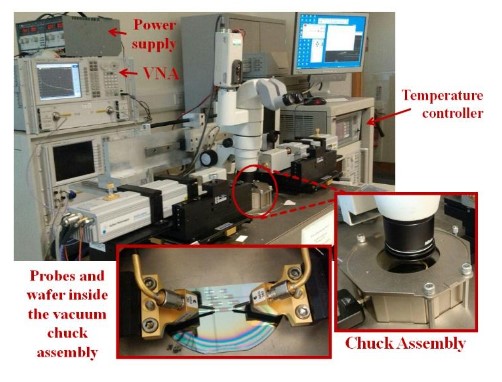
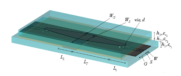
Fig. 1 Test Setup for the temperature- controlled measurements including the chuck assembly and the sample wafer inside.

Download here

Chia sẻ0
Tweet
Chia sẻ

Leave a Reply Cancel reply

Your email address will not be published. Required fields are marked *

Other Posts

Fig. 1 Perspective view of the structure of measurement LC cell

Characterisation and application of nematic liquid crystals in microwave devices

In-Vessel Resonant Communications

Performance Estimation of In-Vessel Resonant Communications

Profile & Bio

Senad Bulja, Ph.D., FIET, SMIEEE 

  1. Dr Bulja’s profile
  2. Email : contact@drbulja.com

PROFESSIONAL Profile

  • Accomplished career of over 19 years demonstrating consistent success as a Researcher, Leader and Mentor in the Wireless industry research environment.
  • Excellent Scientific contributions in the field of RF, EMC and telecommunications with 4 Nature Journal publications and over 70 peer-reviewed articles and conference papers
  • Strong leadership skills demonstrated by leading Ph.D. level educated cross-continental and cross-departmental teams to successful project execution.  
  • Proven Strategic Business Impact – introduced own developed technology into Nokia’s future technology roadmap (RF filters) and business transfer of the smart surface technology. 
  • Creative, internationally awarded and well-driven inventor with over 70 filed patents in the area of hardware for Radio Frequency (RF), Wireless Sensor Networks (WSN), Internet of Things (IoT) and wireless systems architectures. E.g. Nokia patent award entitled: “A top inventor in implementation patent first filings”, 2020.
  • Significant contribution in the identification of high revenue IP assets and leadership on the creation of Nokia’s patent portfolio roadmap. 
 

© Copyright 2023 drbulja.com. All Rights reserved