
In our previous paper on Electro-Chromic (EC) materials, we have shown that standard inorganic EC structures in the form of EC film/electrolyte/Ion storage films (such as WO3/LiNbO3/NiO), in addition to possessing reconfigurable optical properties also exhibit a degree of electric field induce dielectric tunability at radio frequencies. The extent of dielectric tunability in those standard EC structures is commensurate with the tunability exhibited by more mature bulk-tuneable technologies, such as Liquid Crystals (LCs), being between 5% and 20% depending on the frequency of operation, the thickness of the individual EC layers (EC films, electrolyte and ion tank).
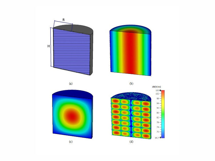
This paper reports on a discovery that the microwave dielectric and the optical characteristics of an EC cell can be engineered to suit a variety of applications without changing their material composition. For this purpose, two inorganic EC cells, differing only in the height of the electrolyte layer (500 nm for cell 1 and 700 nm for cell 2), are used. The thicknesses of the remaining constituent chromic layers of the EC cell, namely WO3 and NiO layers, were chosen in accordance with our previous work [1]. In this study, the respective thicknesses of these layers are hWO3 = 130 nm and hNiO = 140 nm. The heights of the LiNbO3 layers for the two different EC cells are hLiNbO3,1 = 500 nm (cell 1) and hLiNbO3,2 = 700 nm (cell 2), which render the overall heights of the two EC cells hEC,1 = hWO3 + hLiNbO3,1 + hNiO = 770 nm (cell 1) and hEC,2 = hWO3 + hLiNbO3,2 + hNiO = 970 nm (cell 2). Fig. 1 shows the schematic and layer distribution.
The high frequency dielectric characteristics of the proposed cells are extracted in a systematic way in the frequency range from 1 GHz to 20 GHz for the non-actuated and actuated states respectively. The extracted dielectric characteristics of the two cells show that the variation in the height of the electrolyte layer did not only result in their relative, percentage change (between non-actuated and actuated states), but also in the changes of their absolute values. In particular, cell 1 exhibits a dielectric tunability of 20.5 % and 4.8 % at frequencies of 1 GHz and 20 GHz respectively. Similarly, cell 2 has a dielectric tunability of 17.7 % and 7.6 % at frequencies of 1 GHz and 20 GHz respectively. Further, the decomposition of the optical responses (absorbance and reflectance) of the two EC cells reveals different colour composition of the cells and different actuation dc bias voltages, Fig. 2.
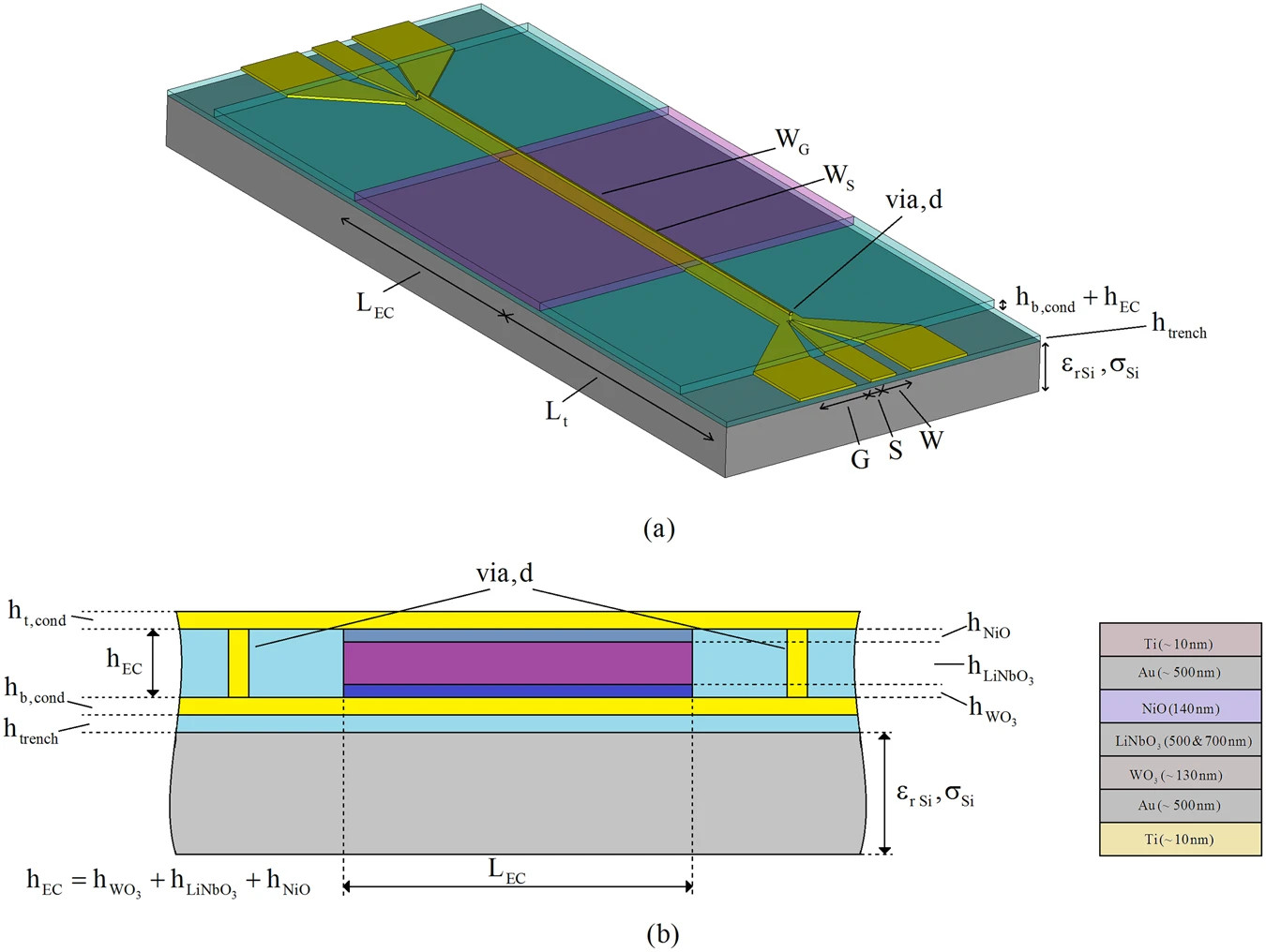
Fig. 1 Schematic of EC measurement device. (a), perspective view. (b), side view and material layer stack
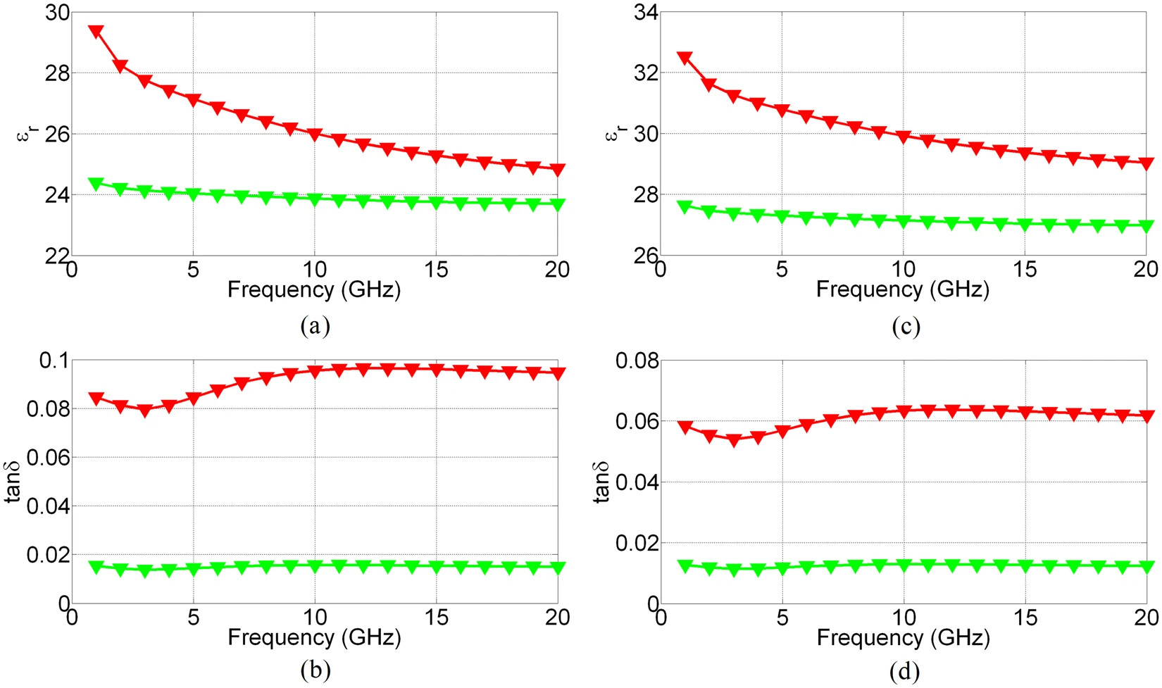
Fig. 2 Decomposition of the optical response of EC cells into R-G-B colour components
Index “min” refers to the normalisation of the recorded minimum intensity of a particular colour component at a prescribed dc bias voltage applied for 6 minutes, index “mean” refers to the normalisation of the recorded average of a particular colour component at a prescribed dc bias voltage applied for 6 minutes and index “end” refers to the normalisation of the recorded end value of a particular colour component at a prescribed dc bias voltage applied for 6 minutes. (a), cell 1, absorption spectrum, (b), cell 2, absorption spectrum, (c), cell 1 reflection spectrum and (d), cell 2 reflection spectrum .
The results presented in this paper indicate that the tunability of both the dielectric permittivity and optical characteristics of EC materials can be tailor made and give rise to the possibility of creation of a new class of devices capable of exploiting the pairing of dielectric and optical effects. There are many examples, ranging from thin displays with a tailor-made optical response and beam-forming function to tuneable optical and microwave devices, such as phase shifters, switches, attenuators and antennas.
Leave a Reply