Dr. Senad Bulja, PhD, FIET, SMIEEE

  • Home
  • Researches
  • Workshops
  • Patents
  • Products
  • Tutorials
  • Solutions
  • Services

Patents

Home » Patents » Apparatus for radio frequency signals and method of manufacturing such apparatus

Apparatus for radio frequency signals and method of manufacturing such apparatus

Dr. Senad Bulja 13/03/2023Download Here

Publication number: 20200313265
Type: Application
Filed: Mar 19, 2020
Publication Date: Oct 1, 2020
Patent Grant number: 11276907
Inventors: Florian Pivit (Dublin), Senad Bulja (Dublin)
Application Number: 16/823,395

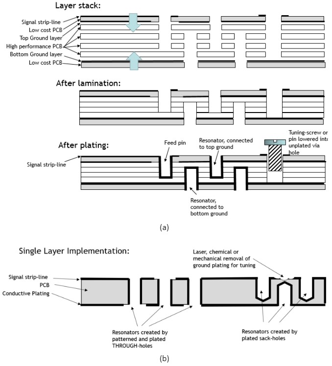
Abstract:  In this invention single and multi-layered PCB distributed resonators and filters implemented in PCB technology are presented.  Fig. 1 depicts how such resonators can be implemented. Distributed resonators and filters have been previously introduced by the author as the means of profile reduction.

Figure 1 Multi-layer PCB implementation (a) and single layer implementation (b) (vertical cross-section through the layer stack), thick black lines representing metalization resp. plating with conductive metal, thin lines representing PCB-layer boundaries)

You may consider: 5G filters 6G filters

Chia sẻ0
Tweet
Chia sẻ

Leave a Reply Cancel reply

Your email address will not be published. Required fields are marked *

Other Posts

Figure 1: moveable active patch on EA based material

Tunable radio-frequency device having electrochromic and electro-active materials 2

Fig. 1. Proposed EA-based smart surface: perspective view showing individual layers in detail

Electroactive material – Controlled smart surface

Fig.1. Block diagram of the modified BFN with reduced number of feeding elements.

Antenna having controlled directivity

Profile & Bio

Senad Bulja, Ph.D., FIET, SMIEEE 

  1. Dr Bulja’s profile
  2. Email : contact@drbulja.com

PROFESSIONAL Profile

  • Accomplished career of over 19 years demonstrating consistent success as a Researcher, Leader and Mentor in the Wireless industry research environment.
  • Excellent Scientific contributions in the field of RF, EMC and telecommunications with 4 Nature Journal publications and over 70 peer-reviewed articles and conference papers
  • Strong leadership skills demonstrated by leading Ph.D. level educated cross-continental and cross-departmental teams to successful project execution.  
  • Proven Strategic Business Impact – introduced own developed technology into Nokia’s future technology roadmap (RF filters) and business transfer of the smart surface technology. 
  • Creative, internationally awarded and well-driven inventor with over 70 filed patents in the area of hardware for Radio Frequency (RF), Wireless Sensor Networks (WSN), Internet of Things (IoT) and wireless systems architectures. E.g. Nokia patent award entitled: “A top inventor in implementation patent first filings”, 2020.
  • Significant contribution in the identification of high revenue IP assets and leadership on the creation of Nokia’s patent portfolio roadmap. 
 

© Copyright 2023 drbulja.com. All Rights reserved