
Passive Inter-Modulation (PIM) is a phenomenon that usually arises in the presence of high-power signals on conducting lines, such as microstrip lines and antennas. Its effects are undesirable as they create signal distortion. This is problematic and unlike active intermodulation taking place on semiconductor devices (diodes and transistors for example) which is well-understood and various techniques exist to combat it, the origin of PIM is not fully understood, making it difficult to properly account for. It is nevertheless strongly linked to high power signals, with the majority of PIM taking place after the main Power Amplifier (PA), usually on the lines connecting the output of the PA and the antennas and, in some cases, antennas themselves. This is troublesome as Digital Pre-Distortion (DPD) techniques, commonly used in the linearization of PA cannot be applied. Over the years, one has developed an understanding that good “housekeeping” helps improve PIM performance, such as ensuring that conducting lines are clean with no visible oxidation, appropriate soldering and avoidance of metal-to-metal contact for the case of dissimilar metals. However, the quest towards a universal solution on how to address PIM still continues.
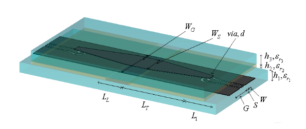
This paper presents new experimental evidence and a novel practical approach for mitigation of PIM in microstrip circuits fabricated on commercial printed circuit board laminates. The mechanisms of distributed PIM in microstrip circuits are reviewed and a phenomenology of PIM generation due to locally enhanced electromagnetic fields at the fringed etched edges of microstrip transmission lines is presented. Reducing the magnitude of the local fields is shown to be an effective means for mitigating PIM distortions. The effect is demonstrated experimentally at frequencies below 1 GHz by selectively coating the edges of a microstrip transmission line with a thin layer (~ 1µm) of high-permittivity dielectric (Ta2O5), which resulted in more than 10 dB reduction of the PIM level without compromising the linear characteristics of the circuit, while avoiding the need for additional signal processing. Our approach has proved to be a new practical and effective means for PIM mitigation suitable for a wide range of commercial printed circuits.

Leave a Reply