
Filters are essential to virtually all communication systems. Even though the fundamental principles of the operation of filters have been known since the second part of the 20th century, practical filter design still draws a great deal of attention from RF engineers and academia. Such is the significance of filters.
Of particular importance to modern filter design is not only excellent electrical performance, but also size and volume. This is principally true for filters operating at the lower end of the frequency spectrum (e.g., 700 MHz), where their physical volume and weight pose significant challenges to network equipment manufactures. In this regard, the need for excellent electrical performance inevitably increases the filter size. Consequently, RF filters tend to occupy a significant volume of a number of communication devices. In particular, cavity filters are still the mainstay in mobile cellular communication base stations, by virtue of their power-handling capabilities, cost effectiveness, good electrical performance (medium to high quality factor) and technological maturity. However, the attractive features of cavity filters are counterbalanced by an increased physical size and, equally importantly, weight. The bulky size can be alleviated at the expense of reduced electrical performance. For example, capacitive loading and a stepped resonant post are often deployed to reduce resonator profile, albeit at the expense of performance. Helical resonators can also be used to address the issue of bulky size.
We have recently introduced a new class of cavity resonators and filters, termed distributed resonators [1] and [2]. The distributed resonator allows a major reduction in the resonator profile while maintaining an excellent electrical performance. In [1], an individual distributed resonator consists of a number of low-profile resonant posts arranged in a grid, where the resonant posts on the vertical and horizontal axes of the grid mainly couple to their immediate neighbors. The substantial reduction in the filter profile, comes – to a degree – at the price of the footprint, mainly due to the fact that the individual distributed resonator consists of a number of resonant posts.
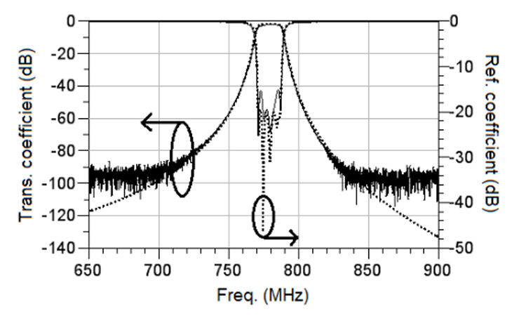
In this paper, multi-layered Print Circuit Board (PCB) distributed resonators and filters are introduced. Here, the individual elements of the distributed resonator are made as part of a multi-layered PCB, commonly used in the circuitry of transceiver (TRX) boards. In this way, the unused real estate available on the board is used effectively. As a demonstrator of the proposed technology, a 2-pole filter fabricated using a 5-layer substrate and consisting of a matrix of 11-by-11 elements per resonator is fabricated and its performance is measured. Due to a large number of individual elements, which perform dimensional averaging of manufacturing inaccuracies, the filter obtained in this way not only requires no post-production tuning, but it also has an extremely low profile of 5o, which is the lowest profile to be reported in the literature. The filter was made to operate at a centre frequency of 1.8 GHz with an absolute bandwidth of 65 MHz. The measured and computed results are in an excellent agreement.
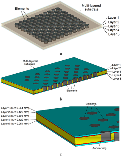
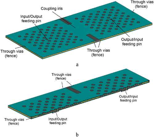
Fig. 1. 11-by-11 multi-layered PCB integrated distributed resonator (left) and designed two-pole multi-layered PCB filter. Housing not shown for clarity.
[1] S. Bulja and M. Gimersky “Low-profile distributed cavity resonators and filters,” accepted for publication in IEEE Trans. Microw. Theory and Techn.
[2] S. Bulja and D. Kozlov, “Split-distributed resonators and filters”, to appear. Presented at Radio and Wireless Symposium, Orlando, US, January 2019.
Leave a Reply