Passive RF components, such as duplexers, filters and antennas, are essential elements of base stations (BS) for wireless communications. Although these components are commonly regarded as linear in low and medium power applications, their behaviour in the systems operating at high-powers exhibits appreciable electrical nonlinearity, which results in the generation of harmonics and spurious intermodulation products. Such a form of intermodulation distortion that occurs in passive components is called passive intermodulation (PIM) [1].
It was experimentally demonstrated that printed circuit board (PCB) components, currently widely used in high power applications, such as radar and telecommunication systems, could be a potential source of unacceptable generation of PIM distortions [2]. From the physical point of view, PIM generation on microstrip circuits is characterized by several important features, such as multiple competing nonlinear sources and their distributed nature. This leads to additional issues during the design and manufacturing process of PCB components and makes their nonlinear properties commonly unpredictable. For these reasons it is of paramount importance to develop new means of PIM mitigation. Preferably, such means should be post-production oriented in order to retain the low cost of PCB manufacture, and also due to the need of retrofitting into existing designs.
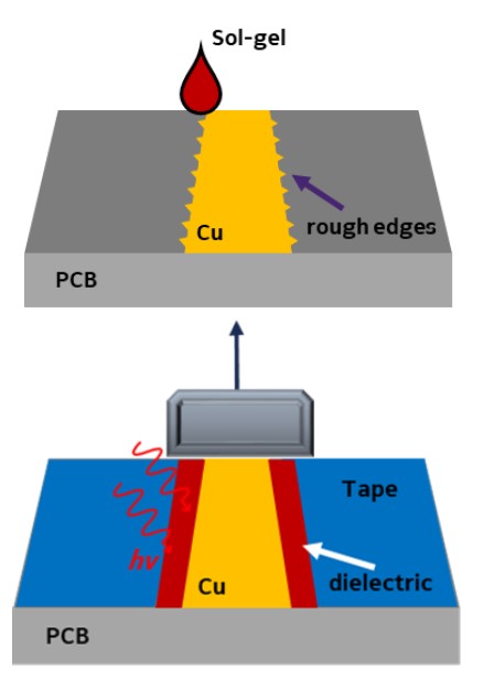
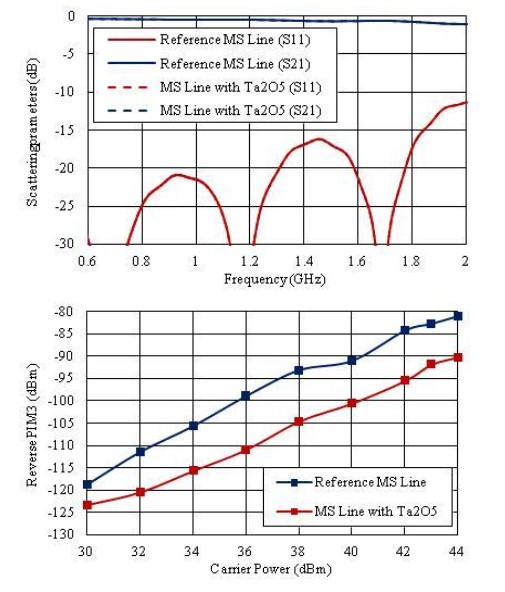
This paper presents a simple technique for effective mitigation of passive intermodulation generated in planar microwave circuits fabricated on commercial printed circuit board laminates. The proposed procedure is based on covering the edges of a microstrip lines with a thin layer of a material of a high dielectric constant, such as tantalum pentoxide (Ta2O5) which reduces the electric field intensity (displacement field) and, hence, nonlinear distortions due to high current density, Fig. 1. The obtained results indicate that an adequate choice of electrical and geometric parameters of the coating dielectric material result in a significant mitigation of passive intermodulation (over 10 dB), while small signal scattering parameters of the measured circuit remain constant, Fig. 2.
[1] P. L. Lui, “Passive intermodulation interference in communication systems,” Electronics & Communication Engineering Journal, vol. 2, no. 3, pp. 109-118, June 1990.
[2] A. G. Schuchinsky, J. Francey and V. F. Fusco, “Distributed sources of passive intermodulation on printed lines,” in Proc. 2005 IEEE Antennas and Propagation Society International Symposium, Washington, DC, 2005, pp. 447-450.
Leave a Reply