
Signal reflections are natural occurrences that take place whenever the propagation environment of a signal changes. Examples of this are evident everywhere – take for example light reflections at the interface of air and water. Such reflections are a consequence of impedance mismatch from the two different propagation environments.
The same principles apply to Electro-Magnetic (EM) waves, since light is, effectively, an EM wave. Every radiated EM signal will get partially reflected and partially transmitted at the interface between media with different propagation environments. This also holds true for microwave circuits, where it is imperative to minimize reflections and, hence, maximize transmission. The extent of reflections in a microwave circuit, Fig. 1, is represented by the reflection coefficient, 𝛤, given by:
(1) 𝛤= (zin-zo)/(zin+zo)
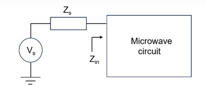
From (1) it can be seen that the lowest level of reflections are achieved when the input impedance of the microwave circuits, , is identical to . Delivering maximum power to any microwave circuit is not only beneficial from the point of view of maximizing the efficiency of the microwave circuit, but, also, from the point of view that high levels of reflections can incur damage to the signal source. This is particularly true for the case of active devices, where unwanted load reflections lead to device instability, unwanted oscillations and, ultimately, device failure.
The design of impedance matching circuits is a well-covered topic in many RF textbooks, such as in [1] and they mostly cover narrow-band impedance matching. Typically, in such approaches either lumped elements or their distributed element counterparts (for high frequencies) are used. However, there exist applications, especially at mm-wave frequencies, where wideband impedance matching is required.
In the next section, as an example, we will design an impedance matching circuit to reduce reflections in a measurement system required to infer unknown dielectric characteristics of a material.
Design of wideband impedance matching circuit
Measurements of unknown dielectric characteristics of a material is a very important task and is required to determine the suitability of use of such a material in microwave circuits. However, measurements of such characteristics are adversely affected by high reflections since in that case very little RF power reaches the material under test and even less RF power reaches the output.
In this example, we will design a broadband impedance matching network for the measurement of dielectric characteristics of Liquid Crystal (LC) mixtures at mm-wave frequencies, 30 GHz to 60 GHz in particular. To this end, we are interested in using a microstrip line structure similar to the one in [2], where the compartment for the LC mixtures in under the microstrip line, as shown in Fig. 2. The width of the microstrip line exposed to the LC compartment is wider than the width of the microstrip at the input and output. The primary reason for this is two-fold. First, in order to adequately capture the behavior of the unknown dielectric characteristics of the LC mixtures, the microstrip line should not be too narrow as this make dielectric parameter extraction less immune to fabrication imperfections, resulting in reduced accuracy and increased uncertainty of the results. Second, the height of the LC compartment is dictated by
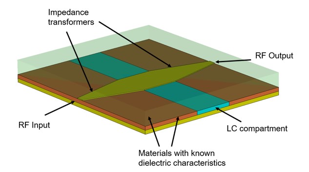
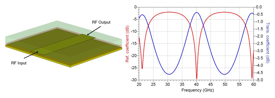
the fact that LC mixtures switching is best observed when substrate heights are not greater than 100 μm, inferring that narrow microstrip lines may not sufficiently well capture the dielectric behavior of the LC mixtures. Due to this, wider microstrip lines are required for the section exposed to LC mixtures, inferring that the corresponding characteristic impedance is quite low. Even though such wide microstrip lines are useful for the characterisation of LC mixtures, the low characteristic impedance and, hence, wide microstrip lines result in impedance mismatch at the input and output, Fig. 3 (a). In the present case, the dielectric permittivity of the bottom and top dielectric materials is and , respectively. With reference to Fig. 3 (a), where the microstrip line is 1 mm wide, this results in a characteristic impedance of approximately 16 Ω, whereas the termination impedance is 50 Ω. The reflection coefficient obtained this way for the length of the line length of 4 mm, is presented in Fig. 3 (b), in the frequency range from 20 GHz to 60 GHz. As can be seen, the return losses exhibit resonant behavior indicating that the line is not matched in an appropriate termination impedance.
To improve impedance match over a wide frequency range, a tapered microstrip line is used. Tapered microstrip lines act as wide-band impedance transformers, provided their electrical length is at least half-wavelength at the lowest frequency of operation. This is depicted in Fig. 4 (a) where one end of the microstrip line is equal to 1 mm, with a characteristic impedance of 16 Ω (wide end) and the other end is narrow with its width equal to 0.19 mm with a characteristic impedance of 50 Ω. The length of the transition section is 2 mm, corresponding to, approximately half-wavelength at a frequency of 30 GHz. The reflection coefficient of the line obtained this way is shown in Fig. 4 (b), in the frequency range from 20 GHz to 60 GHz. As can be seen, excellent impedance matching of lower than -11 dB is achieved over the frequency
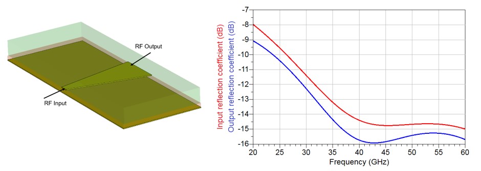
range 30 GHz to 60 GHz. This allows for over 90 % of the total input power to reach the LC compartment. Since the measurements are concerned with the extraction of the unknown dielectric parameters of LC mixtures, the effect of the transitions will need to be taken into account. This can be readily performed using the procedure developed in [3]. As a matter of fact, transitions developed in this way are widely used in the broadband characterisation of unknown dielectric materials. Examples include the measurement of LC mixtures in [3], Electro-Chromic (EC) materials [4], [5], Transition Metal Oxides, [6] and many others.
References:
[1] D. M. Pozar, “Microwave Engineering”, fourth edition, 2011.
[2] S. Bulja and D. Mirshekar-Syahkal, “Novel wideband transition between coplanar waveguide and microstrip line”, IEEE Trans. Microwave Theory and Tech., vol. 58, issue 7, pp.1851-1857, 2010.
[3] S. Bulja, D. Mirshekar-Syahkal, M. Yazdanpanahi, R. James, F. A. Fernandez and S. E. Day, “Measurement of dielectric properties of nematic liquid crystals at milimeter wavelength”, IEEE Trans. Microwave Theory and Tech., vol. 58, issue 12, 3493-3501, 2010.
[4] S. Bulja, R. Kopf, A. Tate & T. Hu “High frequency dielectric characteristics of Electro-chromic, WO3 and NiO films with LiNbO3 electrolyte”, in Nature, Scientific Reports, June 2016.
[5] S. Bulja, R. Kopf, K. Nolan, R. Lundy, A. Tate, T. C. Hu, M. Norooziarab, R. Cahill and W. Templ, “Tuneable dielectric and optical characteristics of tailor-made inorganic electro-chromic materials”, in Nature, Scientific Reports, October 2017.
[6] S. Bulja et al., “High frequency resistive switching behavior of amorphous TiO2 and NiO”, in Nature Scientific Reports, August 2022, https://doi.org/10.1038/s41598-022-16907-8.

Leave a Reply