
Variable attenuators are widely used in modern telecommunication systems, such as in radar systems, point-to-point radio, smart antennas and Radio Frequency (RF) signal cancellation, to name a few. The choice of the attenuator for a particular application is influenced by many factors; for example, the amount of the dynamic range, the insertion losses, power consumption, linearity and power handling capability. For lower power handling capabilities and lower costs, the variation of attenuation is usually achieved using either PIN diodes or FETs [1-2] as active devices, chiefly implemented in the reflection type configuration. The dynamic range of Reflection-type Attenuators (RTAs) is influenced by the parasitic elements of the active device, namely parasitic resistance, lead inductance and parasitic capacitances. These parameters are, ultimately, technology dependent since a more expensive semiconductor technology and better encapsulation of the bare die will inevitably yield lower values of the parasitic elements. Nevertheless, regardless of the technology, a single active device per reflective load is unlikely to yield a dynamic range better than 10-20 dB. In a similar way, insertion losses lower than 1 dB are highly unlikely in standard RTAs. For a greater dynamic range, one can consider several options. The most obvious option lies with a cascade connection of several RTAs, but that would lead to the n-fold increase in the insertion losses. Other options lie with either resorting to the use of different attenuator topologies or using lower parasitic elements active devices. However, both solutions inevitably lead to the increase in the cost.
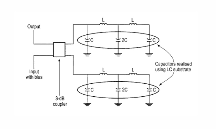
In this paper, we introduce an RTA that is capable of doubling the dynamic range of standard RTAs, without doubling the insertion losses. The proposed RTA consists of a 3-dB coupler and two PIN diodes per reflective load. The PIN diodes are connected to the 3-dB coupler through a network comprising impedance transformers. The exact values of the impedance transformers needed for a high dynamic range are set in accordance with our own developed theory. As an experimental verification, two RTAs have been fabricated – one with a single PIN diode per load and one with the proposed two PIN diodes per load. It is shown that the proposed RTA consisting of two PIN diodes per load offers a dynamic range that is two times greater than its single PIN diode counterpart, without a noteworthy increase in the insertion losses, Fig.1. Both RTA are made to operate at a frequency of 2.1 GHz.
 and Attenuation at 2.1 GHz versus current per diode of single and proposed double load RTAs (right)")
[1] L. M. Devlin and B. J. Minnis. “A versatile vector modulator design for MMIC,” in IEEE M7T-S Int. Symp. Dig., pp. 519-522, 1990.
[2] W. Kang, I. Chang, and M. Kang,“ Reflection-Type Low-Phase-Shift Attenuator”, IEEE Trans. Microw. Theory Techn., vo. 46 no. 7, pp.1019-1021, 1998.
Leave a Reply