
Patent number: 10903568
Type: Grant
Filed: Nov 20, 2018
Date of Patent: Jan 26, 2021
Patent Publication Number: 20200161759
Assignee: NOKIA TECHNOLOGIES OY (Espoo)
Inventors: Senad Bulja (Dublin), Rose Kopf (Greenbrook, NJ), Robert Cahill (Jordanstown), Majid Norooziarab (Blanchardstown)
Primary Examiner: Harry K Liu
Application Number: 16/196,517
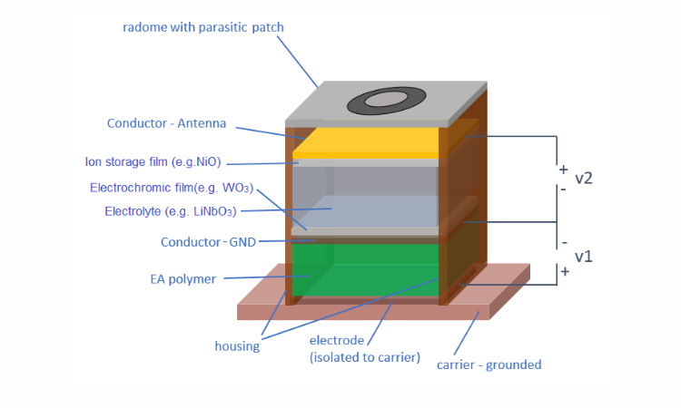
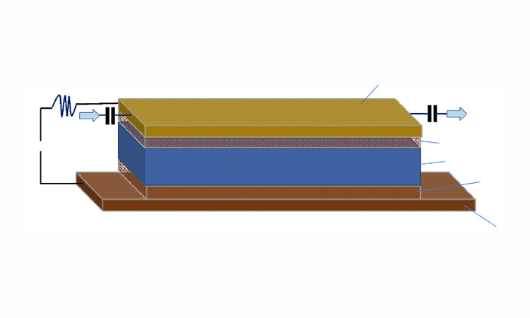
In this invention a patch antenna and a reflect-array based on Electro-Chromic (EC) material is disclosed. The basic structure of the reflect-array unit cell is shown in Fig. 1 and the designed reflect-array operating at 300 GHz using the unit cell of Fig. 1 is shown in Fig. 2.
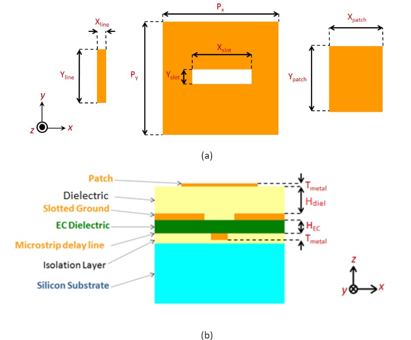
Fig. 1 Topology of the EC- based aperture- coupled reflectarray unit cell (not to scale), (a) front view and (b) side view. The substrate for the patch can be any suitable dielectric such as SiO2 or BCB. The delay line is etched in the isolation layer, however, it is shown as a separate entity. The isolation layer can be any suitable dielectric such as SiO2 , SiN, BCB, to name but a few.
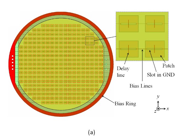
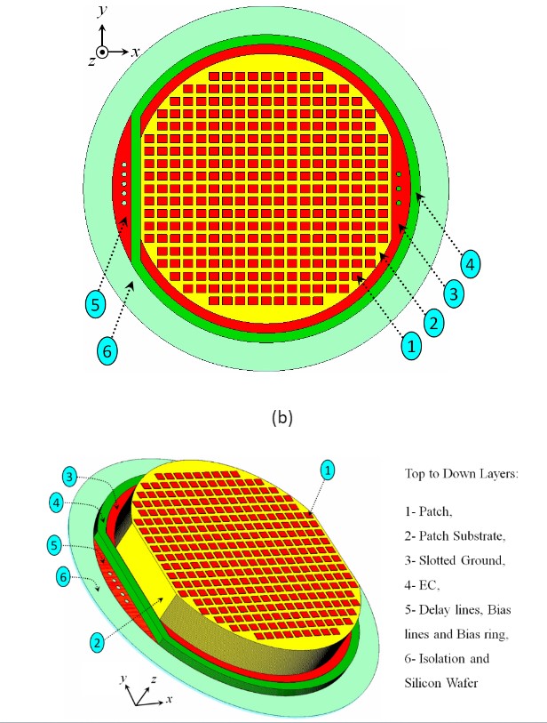
Fig. 2 prototype of the EC reflectarray, fabrication layout (not to scale). (a) Detailed transparent view of the reflectarray (the ground plane is only shown by the slots), (b) Top view and (c) Side view with the sequence of the layers from top to bottom. Also shown is the isolated silicon wafer. The vias on the wafer sides are used to help identify coordinates which is necessary while soldering and setting up the structure in the measurement jig.
Leave a Reply