Dr. Senad Bulja, PhD, FIET, SMIEEE

  • Home
  • Researches
  • Workshops
  • Patents
  • Products
  • Tutorials
  • Solutions
  • Services

Patents

Home » Patents » Electrochromic switch

Electrochromic switch

Dr. Senad Bulja 13/03/2023Download Here

Patent number: 10187107
Type: Grant
Filed: Apr 23, 2018
Date of Patent: Jan 22, 2019
Assignee: Nokia Solutions and Networks Oy (Espoo)
Inventors: Senad Bulja (Dublin), Rose Kopf (Greenbrook, NJ)
Primary Examiner: Blane Jackson
Application Number: 15/959,564

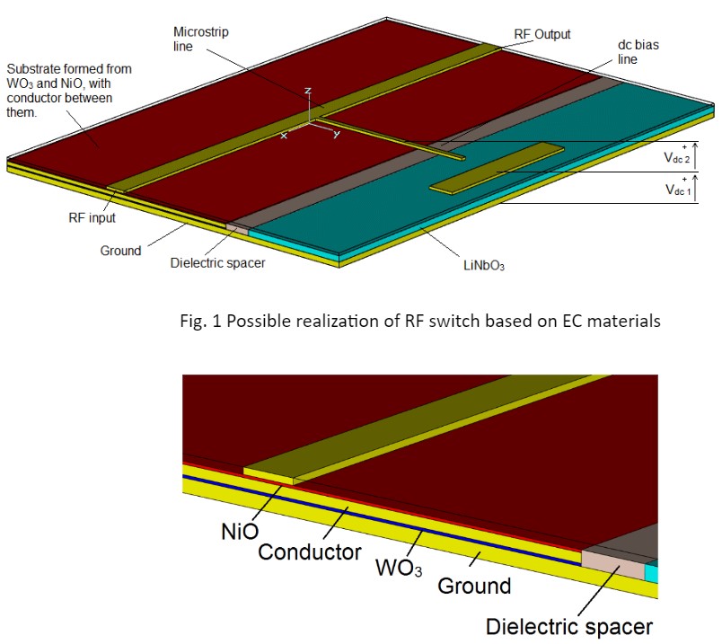
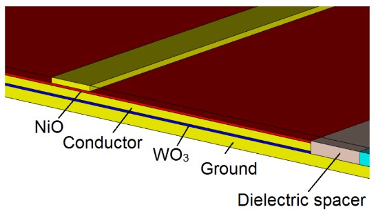
In this invention a switch based on EC materials is presented, its structure is shown in Figs. 1 and 2.  Fig. 1 shows one realisation of an RF switch using EC materials. It consists of a microstrip line mounted on a substrate formed using WO3 and NiO sandwiching a conductor, as shown in Fig.2.  The microstrip line is connected to a DC bias using a high impedance (narrow line). The bias line extends over the EC substrate, the dielectric spacer and reaches the LiNbO3 substrate. Mounted on the LiNbO3 substrate is a conductive pad. In the absence of any dc bias voltage, the microstrip line behaves as a simple transmission line, however, its character changes upon the application of dc bias. 

Two dc bias voltages are necessary for the operation of the microstrip line as a switch. Vdc1 is applied between the conductive pad and the ground plane in order to set the LiNbO3 ions in motion. Once in motions, these ions, by virtue of Vdc2 are moved towards the RF microstrip line, where they subsequently get injected into the chromic layers (WO3 and NiO). Upon intercalation the chromic layers become conductive, which short-circuits them with the middle conductor. Now, the microstrip line is entirely short circuited, which is needed for the correct operation of the switch. 

Fig. 1 Possible realization of RF switch based on EC materials
Fig. 2 Close-up view of microstrip line substrate

Chia sẻ0
Tweet
Chia sẻ

Leave a Reply Cancel reply

Your email address will not be published. Required fields are marked *

Other Posts

Figure 1 Exemplarily embodiments of PMF based RF splitting/switching device, enabled by TMO or EC material (a) and Exemplarily embodiment of air cavity waveguide-based RF splitting/switching device, enabled by TMO or EC material (b)

Controllable radio frequency switching and/or splitting device

equivalent circuit for implicit coupling among replicated resonators

Radio communications

Figure 1: All exemplary Wi-Fi operation states

Filtration for radio access technologies

Profile & Bio

Senad Bulja, Ph.D., FIET, SMIEEE 

  1. Dr Bulja’s profile
  2. Email : contact@drbulja.com

PROFESSIONAL Profile

  • Accomplished career of over 19 years demonstrating consistent success as a Researcher, Leader and Mentor in the Wireless industry research environment.
  • Excellent Scientific contributions in the field of RF, EMC and telecommunications with 4 Nature Journal publications and over 70 peer-reviewed articles and conference papers
  • Strong leadership skills demonstrated by leading Ph.D. level educated cross-continental and cross-departmental teams to successful project execution.  
  • Proven Strategic Business Impact – introduced own developed technology into Nokia’s future technology roadmap (RF filters) and business transfer of the smart surface technology. 
  • Creative, internationally awarded and well-driven inventor with over 70 filed patents in the area of hardware for Radio Frequency (RF), Wireless Sensor Networks (WSN), Internet of Things (IoT) and wireless systems architectures. E.g. Nokia patent award entitled: “A top inventor in implementation patent first filings”, 2020.
  • Significant contribution in the identification of high revenue IP assets and leadership on the creation of Nokia’s patent portfolio roadmap. 
 

© Copyright 2023 drbulja.com. All Rights reserved