Dr. Senad Bulja, PhD, FIET, SMIEEE

  • Home
  • Researches
  • Workshops
  • Patents
  • Products
  • Tutorials
  • Solutions
  • Services

Patents

Home » Patents » Apparatus Comprising a First and Second Layer of Conductive Material and Methods of Manufacturing and Operating Such Apparatus

Apparatus Comprising a First and Second Layer of Conductive Material and Methods of Manufacturing and Operating Such Apparatus

Dr. Senad Bulja 13/03/2023Download Here

Publication number: 20200076221
Type: Application
Filed: Aug 28, 2019
Publication Date: Mar 5, 2020
Patent Grant number: 11309729
Inventors: Senad Bulja (Dublin), Pawel Rulikowski (Dublin), Anna Wielgoszewska (Dublin)
Application Number: 16/553,857

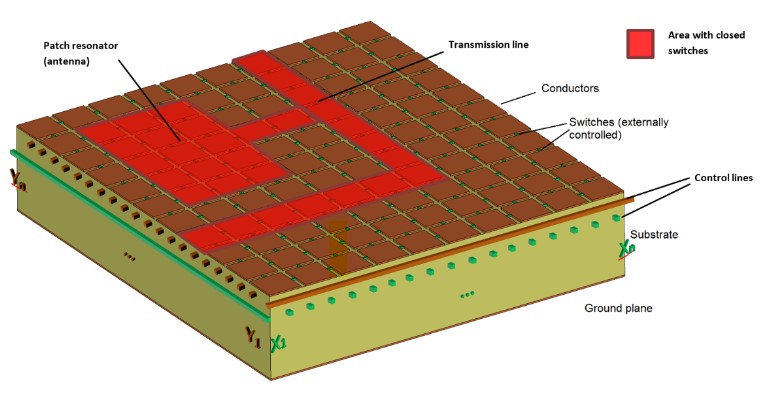
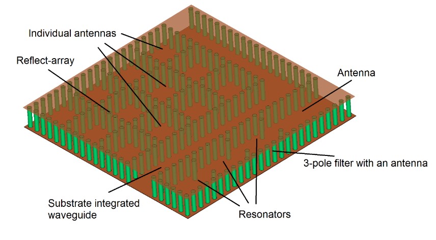
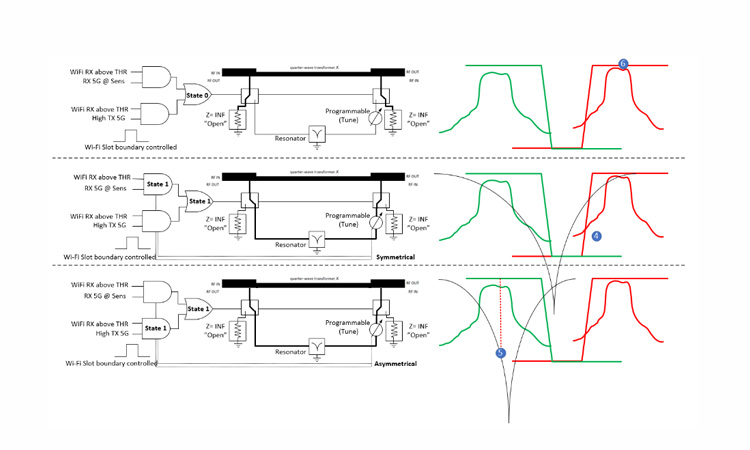
Abstract:  In this invention a programmable 2D and 3D technologies are introduced, realized either in the form of adaptive surfaces or volumes. Ax example of a programmable 2D technology is shown in Fig. 1 and programmable volumes in Fig. 3.

Fig. 1 Illustration of a circuit created by 2D programmable surface
Fig. 1 Illustration of a circuit created by 3D programmable volume

Chia sẻ0
Tweet
Chia sẻ

Leave a Reply Cancel reply

Your email address will not be published. Required fields are marked *

Other Posts

Figure 1 Exemplarily embodiments of PMF based RF splitting/switching device, enabled by TMO or EC material (a) and Exemplarily embodiment of air cavity waveguide-based RF splitting/switching device, enabled by TMO or EC material (b)

Controllable radio frequency switching and/or splitting device

equivalent circuit for implicit coupling among replicated resonators

Radio communications

Figure 1: All exemplary Wi-Fi operation states

Filtration for radio access technologies

Profile & Bio

Senad Bulja, Ph.D., FIET, SMIEEE 

  1. Dr Bulja’s profile
  2. Email : contact@drbulja.com

PROFESSIONAL Profile

  • Accomplished career of over 19 years demonstrating consistent success as a Researcher, Leader and Mentor in the Wireless industry research environment.
  • Excellent Scientific contributions in the field of RF, EMC and telecommunications with 4 Nature Journal publications and over 70 peer-reviewed articles and conference papers
  • Strong leadership skills demonstrated by leading Ph.D. level educated cross-continental and cross-departmental teams to successful project execution.  
  • Proven Strategic Business Impact – introduced own developed technology into Nokia’s future technology roadmap (RF filters) and business transfer of the smart surface technology. 
  • Creative, internationally awarded and well-driven inventor with over 70 filed patents in the area of hardware for Radio Frequency (RF), Wireless Sensor Networks (WSN), Internet of Things (IoT) and wireless systems architectures. E.g. Nokia patent award entitled: “A top inventor in implementation patent first filings”, 2020.
  • Significant contribution in the identification of high revenue IP assets and leadership on the creation of Nokia’s patent portfolio roadmap. 
 

© Copyright 2023 drbulja.com. All Rights reserved