Dr. Senad Bulja, PhD, FIET, SMIEEE

  • Home
  • Researches
  • Workshops
  • Patents
  • Products
  • Tutorials
  • Solutions
  • Services

Patents

Home » Patents » Antenna having controlled directivity

Antenna having controlled directivity

Dr. Senad Bulja 15/03/2023Download Here

Publication number: 20200411988
Type: Application
Filed: Jun 24, 2020
Publication Date: Dec 31, 2020
Applicant: NOKIA SOLUTIONS AND NETWORKS OY (Espoo)
Inventors: Dimitry KOZLOV (Dublin), Senad BULJA (Dublin), Jack MILLIST (Carcassonne)
Application Number: 16/910,299

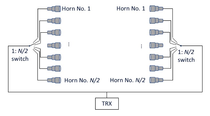
Abstract:  The basic idea of the present invention submission lies with the modification of a lens antenna Beam-Forming Network (BFN) by dividing the feeding elements into two separate groups and simultaneous excitation of two elements – one from each group. This should be done in the way that any element of the first and second groups can be chosen independently at any instant. This can be achieved by using two independent switching networks connected to the feeding elements (Fig. 1). As one can see, such a BFN allows us to create N2/4 different radiation patterns (RP) by a sequential combination of N/2 elements from the first group and N/2 elements from the second one. It is obvious that N2/4 > N if N>4 and this difference quadratically increases as a function of N. Alternatively, if the directions of the potentially created beams are fixed, the number of feeding elements can be reduced.

The proposed approach is based on the fact that a radiation pattern (RP) of a lens antenna, created by a simultaneous activation of two individual feeding elements represents a superposition of two individual RPs, created by independent excitation of these elements. Thus, the direction of the beam is defined by spatial coordinates of both feeding elements.

Fig.1. Block diagram of the modified BFN with reduced number of feeding elements.

You may consider: 5G filters 6G filters

Chia sẻ0
Tweet
Chia sẻ

Leave a Reply Cancel reply

Your email address will not be published. Required fields are marked *

Other Posts

Figure 1: moveable active patch on EA based material

Tunable radio-frequency device having electrochromic and electro-active materials 2

Fig. 1. Proposed EA-based smart surface: perspective view showing individual layers in detail

Electroactive material – Controlled smart surface

Figure 1 Multi-layer PCB implementation

Apparatus for radio frequency signals and method of manufacturing such apparatus

Profile & Bio

Senad Bulja, Ph.D., FIET, SMIEEE 

  1. Dr Bulja’s profile
  2. Email : contact@drbulja.com

PROFESSIONAL Profile

  • Accomplished career of over 19 years demonstrating consistent success as a Researcher, Leader and Mentor in the Wireless industry research environment.
  • Excellent Scientific contributions in the field of RF, EMC and telecommunications with 4 Nature Journal publications and over 70 peer-reviewed articles and conference papers
  • Strong leadership skills demonstrated by leading Ph.D. level educated cross-continental and cross-departmental teams to successful project execution.  
  • Proven Strategic Business Impact – introduced own developed technology into Nokia’s future technology roadmap (RF filters) and business transfer of the smart surface technology. 
  • Creative, internationally awarded and well-driven inventor with over 70 filed patents in the area of hardware for Radio Frequency (RF), Wireless Sensor Networks (WSN), Internet of Things (IoT) and wireless systems architectures. E.g. Nokia patent award entitled: “A top inventor in implementation patent first filings”, 2020.
  • Significant contribution in the identification of high revenue IP assets and leadership on the creation of Nokia’s patent portfolio roadmap. 
 

© Copyright 2023 drbulja.com. All Rights reserved