The quality of computation in any domain (digital or analogue) rests on the ability of its fundamental components to change some of their characteristics under an external influence. From the aspect of digital computation, the transistor was used as a switch (bit), able to perform computation as part of a much larger set of transistors. The computation performed in this way operated on quantized or digital waveforms, with analogue signals converted into the digital domain using Analogue to Digital Converters (ADC). Here, the role of a switch was simply to occupy a simple “0” or “1” state. The response of the set of transistors, i.e. bits is then converted to an equivalent analogue waveform (Digital to Analogue Converter) for display purposes. The question as to whether all computation could be performed on analogue waveforms without the need for conversion to digital domains can be posed? To an extent this was achieved in the past, where typically, operational amplifiers with external active and passive circuitries were used as the main building blocks[i], [ii]. Even though such analogue computers were fast, digital computers proved more versatile which led to their greater spread[iii]. However, with the advent of new 6G technologies where the main drivers include flexible spectrum usage (reconfigurability) and low latency[iv],[v],[vi], [vii], [viii], [ix], another question may be posed as to whether analogue computing needs to be revisited? This, coupled with the discovery of new materials, capable of reversible and fast phase change, appears to be an interesting prospect. Such an analogue computing device will be capable of performing a variety of operations directly on radio signals to enable ultrafast processing and communications. To enable versatility of such analogue radio signal computing devices, the active material needs to be in bulk form, i.e. able to be deposited on almost arbitrary-shapes or surfaces and volumes. Taken very broadly, this has already been performed in the form of reconfigurability enablement, where reconfigurability was supported by the ability of the active element to change certain aspects of RF/mm-wave components. In the case of RF filters and antennas, this was typically the frequency of operation and/or bandwidth[x] or in certain other instances, the radiation characteristics[xi]. However, this does not constitute computing in the traditional sense.
Bulk-tuneable materials have been, to an extent, used to enable reconfigurable radio components, even though such efforts are still in technological infancy, despite being around for a very long time. The most widely examined bulk-tuneable materials include Liquid Crystals (LCs)[xii],[xiii], [xiv] , Ferro-Electrics (FE)[xv], [xvi], [xvii] and, most recently, the pioneering work on Electro-Chromic (EC) materials[xviii], [xix], [xx], [xxi], [xxii],[xxiii],[xxiv], proving the link between optical and electrical characteristics. However, these materials have not yielded a great deal of commercial traction, because electrical and size requirements imposed on commercially available RF and mm-wave hardware are very strict and simply cannot be met using the reconfigurable technologies available today. For example, the loss tangents of LC mixtures still tend to be quite large – of the order of 0.03xiii, which is considered too large for many applications, while their response time is usually of the order of a few msxii. FEs, even though offering larger tuneable ranges than LCs exhibit very high dielectric constants which are of limited use for RF and mm-wave applications. The research on EC materials is still in infancy, however it appears to offer a compromise between the LCs and FEs, with an added benefit of exhibiting a strong memory effect. The devices and architectures that these traditional bulk-tuneable materials can support in the context of future networks is therefore limited to niche devices encompassing phase shifters, attenuators, to name but a few, where the integration with semiconductor technologies is easier.
However, recently there has been a great deal of progress towards the use of Resistive Switching (RS) exhibited by a new type of bulk controllable material, Transition Metal Oxides (TMOs)[xxv],[xxvi]. Several TMOs have been investigated, such as VOx[xxvii], TiO2[xxviii] , NiO[xxix], SrTiO3[xxx] to name but a few as bulk switching elements. The oxides of vanadium have been found to offer excellent electrical performance at mm-wave frequencies[xxxi], [xxxii], [xxxiii], [xxxiv], [xxxv]. As an example,[xxxvi], a 200 nm thick VO2 layer deposited using reactive laser ablation on a CPW (Coplanar Waveguide) to form series and parallel switch configurations, was characterised from 5 GHz to 35 GHz. The achieved dynamic range observed is of the order of 25 dB with an insertion loss of about 0.8 dB. The switching speed of VOx is highly dependent on the deposition technique and is reported to be in the range of several ns down to ps[xxxvii], [xxxviii], [xxxix] . Characterisation of TMOs other than VOx and their use in the context of RF & mm-wave devices has been virtually unexplored due to technological delay in responding to demands for very low-power, low-cost and very fast non-semiconductor switches, apart from the work by Bulja which reported on the characterisation of amorphous WO3, TiO2 and NiO as a function of the dc bias[xl]. In any case, TMOs appear to hold the promise of cost effectiveness while at the same time being able to be deposited on almost arbitrary surfaces, using different printing techniques, such as inkjet printing[xli],[xlii]. It is of further importance to mention the possibility of inducing bulk-material tunability based on bulk-material switches (TMOs), as shown by Bulja[xliii]. From this aspect, a question could be posed as to whether these new materials could be utilized in the context of novel ways of computing? And more specifically, will novel computing ways utilize bulk-material switches or bulk dielectric tunability? How would such a structure look like?
A possible answer to that question lies with Intelligent Surfaces (IS). To this end, IS have attracted a great deal of attention recently, since they allow the attainment of re-configurability, which is of great importance in the context of 5G and upcoming 6G and beyond specifications. In particular, IS in the form of Intelligent Reflective Surfaces (IRS) have been used to mitigate harmful effects of the wireless environment by their virtue and ability to redirect incoming signals towards a specific path. This ability is usually achieved by controlling some parameters of meta-atoms, such as the phases and amplitudes. The controlling elements can be managed through either a semi-conductor device, Micro-Electro-Mechanical Switch (MEMS) or LCs[xliv], depending on the parameter of the meta-atoms that are being controlled. In turn, this allows the IRS to manipulate the incident wavefront to achieve steering, adjustable absorption, polarisation, filtering and collimation[xlv]. However, the losses and latency times of the constituent materials limit their application range[xlvi]. Given this premise of IS, it is only natural to ask if the combination of new bulk switchable materials (TMOs in this case) and IS, could lead to the creation of new types of reconfigurabilities, namely computation in the natural domains of radio signals? This will sufficiently take advantage of the very nature of IS, create new ways of computation and act as an enabler of 6G technologies. Let us explore how this could possibly be implemented.
Analogue computing – Implementation
To perform spatial computation on a radio signal impinging on an arbitrary surface, it is imperative to have adequate control of the dielectric characteristics of such a medium with granularity that is commensurate with the wavelength at which computation is to be performed. In computational Electro-Magnetics (EM), reasonable accuracy is achieved using at least 10 cells for a given wavelength, with higher accuracies possible with a denser mesh. It was shown that the control of dielectric permittivity and magnetic permeability of a medium allows for control of functionality of such a medium[xlvii], [xlviii]. To this end, the concept of digital metamaterial bits was introduced in[xlix], where it was shown that using two EM
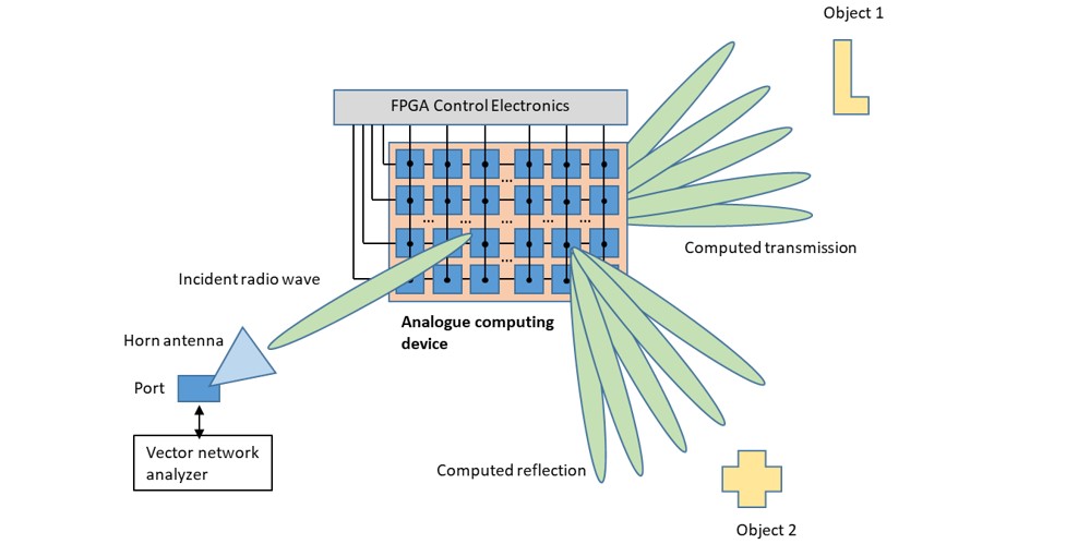
Fig. 1: Schematic depiction of an experimental setup to demonstrate analogue computation on radio waves, realizing a single-frequency, single-antenna object imaging system (in transmission and/or reflection)[i]
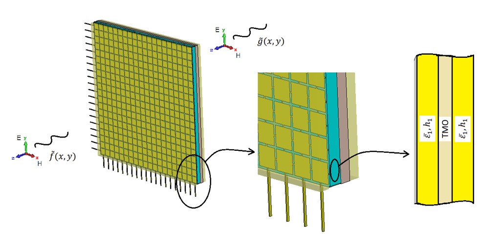
metamaterials, one can synthesize an EM metamaterial with desired dielectric properties at a given frequency of operation. This concept opened a new way of perceiving metamaterials, which led to the extension of the concept to variable, coding metamaterialsl, ultimately used to control the radiation characteristics of a smart surface. The realisation that metamaterials with a pre-described dielectric permittivity can be used to perform mathematical operations, was already shown[i], [ii], however it was only for static cases. For a medium to perform arbitrary mathematical operations, the static case is of little value. To perform an arbitrary mathematical operation, the dielectric permittivity of the medium needs to be externally controllable to a local level and to yield a dielectric permittivity distribution across the entire medium. This is only achievable using bulk reconfigurable materials, such as TMOs mentioned earlier. The exact physical realizations of such devices are difficult to predict at this stage, however, one possible realization is shown in Fig. 2, which indicates that the radio signal incident on the structure, will emerge altered on the other end of the structure as . The extent of change of the incident signal is proportional to the distribution of the dielectric characteristics across the structure. As the means of enabling dielectric reconfigurability, TMO inspired structures can be used. As an example, the extent of dielectric reconfigurability can be maximized by interlacing dielectrics and sub-skin depth TMO, as shown in an earlier concept introduced by Buljaxliii.
Each pixel (cell) of Fig. 2 will consist of such an interlaced dielectric-TMO- dielectric structure, will be individually addressable and be able to change its constituent parameters (composite dielectric permittivity) upon actuation (application of dc bias voltage). The highest frequency of operation, , of structures obtained in this way will be dictated by pixel resolution, i.e. number of cells per wavelength and the dielectric characteristics of the medium obtained using the following formula:

Here, c stands for the velocity of light, for the composite relative dielectric permittivity and stands for the number of cells at the upper frequency of operation. Since reasonable accuracy in computational EM is obtained using at least 10 cells per wavelength and that the macroscopic dielectric permittivity of standard dielectrics is around , it becomes possible to estimate the upper frequency of operation of structures obtained in this way. For a resolution of 1 mm, the highest frequency of operation becomes 17.3 GHz, whereas for the case of ultra-precise 3D printing resolution of 5 μm, the highest frequency of operation becomes 3.46 THz. However, these are estimates only and that the final values will be decided upon testing and evaluating the extent of dielectric reconfigurability in interlaced TMO structures. The extent of dielectric reconfigurability will be dependent on the examined TMO, the dielectric carrier substrate and their corresponding thicknesses.
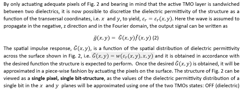
and ON (metallic). Possibilities exist to extend the concept to multi-layered or stacked structures, expected to provide a greater granularity of achievable dielectric permittivities across the surface.
It needs to be understood that the concept this is a concept only and there are many unknowns as to how the proposed solution will work. For example, there exist serious questions regarding how one can bias such structures, the palette of mathematical functions one will be able to perform using the structure and the extent of signal reflections taking place at the boundary of the surface. At present, there are no answers to this, and this article does not intend to provide them in any case.
Summary
This article reviewed analogue computing and presented a vision of how, in the context of advanced 5G and forthcoming 6G applications and advancements in the development of new materials, analogue computing performing mathematical operations directly on radio signals is worth investigating. In doing so, the article provided a brief historical aspect on analogue computing, reviewed the current state-of-the art of bulk-reconfigurable materials, IS and the current structures used to perform “static” computation directly on radio signals. Based on this and through a thought experiment, the article proposed new structures capable, at least in principle, of performing a palette of mathematical functions in a dynamic fashion. In doing so, the article aims to challenge the traditional way of thinking, approaching and solving problems, leading to the ultimate realization that computing can be performed by anything and anywhere.
References
[1] C.Bissell, “A great disappearing act: the electronic analogue computer”, IEEE Conference on the History of Electronics, Bletchley Park, UK, 28-30 June 2004.
[1] J. S. Small, “The analogue alternative: the electronic analogue computer in Britain and the USA, 1930-1975”, 1st edition, September 2001, London, UK.
[1] I. B. Pyne, “Linear programming on an electronic analogue computer”, in Transactions of the American Institute of Electrical Engineers, Part I: Communication and Electronics, vol. 75, issue: 2, May 1956.
[1] Ericsson, white paper, “6G-Connecting a cyber-physical world”, https://www.ericsson.com/en/reports-and-papers/white-papers/a-research-outlook-towards-6g.
[1] H. Viswanathan and P. E. Mogensen, “Communications in the 6G era”, in IEEE Access, vol. 8, 2020.
[1] NTT DOCOMO, White paper, “5G evolution and 6G”: https://www.docomo.ne.jp/english/binary/pdf/corporate/technology/whitepaper_6g/DOCOMO_6G_White_PaperEN_v4.0.pdf.
[1] White paper, 6g Flagship, University of Oulu, “ RF-enabling 6G Opportunities and challenges from technology to spectrum”, 6G Research Visions, no. 13, April 2021.
[1] O. Al-Saadeh, G. Wikstrom, J. Sachs, I. Thibault and D. Lister, “End-to-end latency and reliability performance of 5G in London”, in IEEE Global Communications Conference (GLOBECOM), 2018.
[1] M. Polese, J. M. Jornet, T. Melodia and M. Zorzi, “Toward end-to-end, full-stack 6G Terahertz Networks”, in IEEE Communications Magazine, vol. 58, Issue 11, Nov. 2020.
[1] M. Yazdanpanahi, P. Deo and D. Mirshekar-Syahkal, “Tunable liquid-crystal millimeter-wave bandpass filter using periodical structure”, in IEEE Radio and Wireless Symposium (RWS), Jan. 2014.
[1] P. Ludlow and V. Fusco, “Reconfigurable small-aperture evanescent waveguide antenna”, in IEEE Transactions on Antennas and Propagation, vol. 59, issue 12, Dec. 2011.
[1] R. James, F. A. Fernandez, S. E. Day, S. Bulja and D. Mirshekar-Syahkal, “Accurate modelling for wideband characterisation of nematic liquid crystals for microwave applications”, in IEEE Microwave Theory and Techniques, pp. 3293-3297, vol. 57, issue 12, 2009.
[1] S. Bulja, D. Mirshekar-Syahkal, R. James, S. E. Day and F. A. Fernandez, “Measurement of dielectric properties of nematic liquid crystals at millimetre wavelength”, in IEEE Microwave Theory and Techniques, pp. 3493-3501, vol. 58, issue 12, 2010.
[1] M. Yazdanpanahi, S. Bulja, D. Mirshekar-Syahkal, R. James, S. E. Day and F. A. Fernandez, “Measurement of dielectric constants of nematic liquid crystals at mm-wave frequencies using patch resonator”, in IEEE Transactions on Instrumentation and Measurement, pp. 3079-3085, vol. 59, issue 12, 2010.
[1] R. R. Romanofsky, “Advances in scanning reflectarray antennas based on ferroelectric thin-film phase shifters for deep space communications”, in Proceedings of the IEEE, pp. 1968-1975, vol. 95, issue 10, 2007.
[1] M. Haghzadeh, C. Armiento and A. Akyurtlu, “All-printed flexible microwave varactors and phase shifters based on a tunable BST/Polymer”, in IEEE Microwave Theory and Techniques, pp. 2030-2042, vol. 65, issue 6, 2017.
[1] M. Nikfalazar, A. Mehmood, M. Sohrabi, M. Mikojalek, A. Wiens, H. Maune, C. Kohler, J. R. Binder and R. Jakoby, “Steerable dielectric resonator phased-array antenna based on inkjet-printed tunable phase shifter with BST Metal-Insulator-Metal varactors”, in IEEE Antennas and Propagation Letters, pp. 877-880, vol. 15, 2015.
[1] Bulja, S., Kopf, R., Tate, A. et al. High Frequency Dielectric Characteristics of Electrochromic, WO3 and NiO Films with LiNbO3 Electrolyte. Sci Rep 6, 28839 (2016)
[1] Bulja, S., Kopf, R., Nolan, K. et al. Tuneable dielectric and optical characteristics of tailor-made inorganic electro-chromic materials. Sci Rep 7, 13484 (2017)
[1] Bulja, S., Kopf, R., Tate, A. et al. Electro-chromic structure with a high degree of dielectric tunability. Sci Rep 9, 10773 (2019).
[1] M. Norooziarab, S. Bulja, R. Cahill, R. Kopf, T. C. Hu and A. Tate, “Variable temperature broadband and millimetre-wave characterisation of electrochromic (WO3/LiNbO3/NiO) thin films”, in IEEE Microwave Theory and Techniques, pp. 1070-1080, vol. 66, issue 2, 2018.
[1] S. Bulja et al., “Electrochromic switch”, Patent, U.S. patent number: 10,187,107.
[1] S. Bulja et al., “Electrochromic reflectarray antenna”, Patent, U.S. patent number: 10,033,080.
[1] S. Bulja et., “Electrochromic cell for radio-frequency applications”, Patent, U.S. patent number: 10,187,107.
[1] F. J. Morin, “Oxides which show a metal-to-insulator transition at the neel temperature,” Phys. Rev. Lett., vol. 3, no. 1, pp. 34–36, Jul. 1959.
[1] A. Sawa et al, “Resistive switching in transition metal oxides”, Materials Today, vol.11, no.6, 2008
[1] A. X. Grays et al., “Correlation-driven insulateor metal transition in nea-ideal vanadium dioxide films”, Phys. Rev. Lett. Vol. 116, 116403, 2016.
[1] C. Rhode, B. J. Choi, D. S. Jeong, S. Choi, J.-S. Zhao, and C. S. Hwang, “Identification of a determining parameters for resistive switching of TiO2 films” Appl. Phys. Lett. 86, 262907, 2005.
[1] P. Misra et al, “Studies on resistive switching times in NiO thin films grown by pulsed laser deposition”, J. Phys. D: Appl. Phys., vol.50, 2017.
[1] K. Szot, W. Speier, G. Bihlmayer and R. Waser, “Switching the electrical resistance of individual dislocations in single-crystalline SrTiO3”, in Nature Materials, vol. 5, doi:10.1038/nmat1614, April 2006.
[1] A Crunteanu et el, “Microwave switching functions using reversible metal-insulator transition (MIT) in VO2 thin films,” Proc. 37th EuMC, Germany, 2007.
[1] J Jiang et al, “Fabrication and characterization of V02-based series and parallel RF switches”, IEEE MTT-S Int Microwave Symp (IMS) Digest, Honolulu, Hawaii, USA, 2017
[1] K C Pan, et al, “Vanadium oxide thin-film variable resistor-based RF switches,” IEEE Trans on Electron Devices, vol. 62, no. 9, 2959-65, Sept. 2015.
[1] Y Zhou et al, “Voltage-triggered ultra-fast metal-insulator transition in vanadium dioxide switches,” IEEE Electron
Device Letters, vol. 34, no. 2, 220-2, Feb. 2013.
[1] L Huitema et al, “Highly integrated VO2 based tunable antenna for millimeter wave applications,” Applied Physics Letters, vol. 110 (20), 203501/1-5, May 2017.
[1] J Jiang et al, “Fabrication and characterization of V02-based series and parallel RF switches”, IEEE MTT-S Int Microwave Symp (IMS) Digest, Honolulu, Hawaii, USA, 2017.
[1] A. Cavalleri, C. S. Tóth, C.W. Siders, J. A. Squier, F. Ráksi, P. Forget and J. C. Kieffer, “Femtosecond Structural Dynamics in VO2 during an Ultrafast Solid-Solid Phase Transition”, Physical Review Letters, 87(23) 237401-1 – 237401-4, 2001.
[1] J Leroy et al, “High-speed metal-insulator transition in vanadium dioxide films induced by an electrical pulsed voltage over nano-gap electrodes,” Appl. Phys. Lett., vol. 100, no. 21, 213507-1–213507-4, 2012.
[1] Z. Yang et al, “Oxide electronics utilizing ultrafast metal-insulator transitions,” Annual Review of Materials Research, vol. 41, no. 1, 337-367, Aug. 2011.
[1] S. Bulja, R. Kopf, A. Tate, M. Cappuzzo, D. Kozlov, H. Claussen, D. Wiegner, W. Templ and D. Mirshekar-Syahkal, “High frequency resistive switching behavior of amorphous TiO2 and NiO”, in Nature Scientific Reports, August 2022, https://doi.org/10.1038/s41598-022-16907-8.
[1] W. Li, M. Vaseem, S. Yang and A. Shamim, “Flexible and reconfigurable radio frequency electronics realized by high-throughput screen printing of vanadium dioxide switches”, in Microsystems & Nanoengineering, (2020)6:77
[1] M. Vaseem, F. A. Ghaffar, M. F. Farooqui and A. Shamim, “Iron oxide nanoparticle-based magnetic ink development for fully printed tunable radio-frequency devices”, in Advanced Materials Technologies, 3, 1700242, 2018.
[1] S. Bulja et el., “Radio-frequency switching apparatus”, Patent, U.S. Patent number: 11,201,634.
[1] C. Huang, S. Hu, G. C. Alexandropoulos, A. Zappone, C. Yuen, R. Zhang, M. Di Renzo, and M. Debbah, “Holographic MIMO surfaces for 6G wireless networks: Opportunities, challenges, and trends,” [Online] Available: https://arxiv.org/abs/1911.12296, accessed on Jan. 2020.
[1] C. Liaskos, S. Nie, A. Tsioliaridou, A. Pitsillides, S. Ioannidis, and I.Akyildiz, “A New Wireless Communication Paradigm through Software-Controlled Metasurfaces,” IEEE Wireless Commun., vol. 56, no. 9, Sep.2018, pp. 162-169.
[1] M. F. Imani, J. N. Gollub, O. Yurduseven, A. V. Diebold, M. Boyarsky, T. Fromenteze, L. Pullido-Mancera, T. Sleasman and D. R. Smith, “Review of metasurface antennas for computational microwave imaging”, in IEEE Transactions on Antenna and Propagation, pp. 1860-1875, vol. 68, no. 3, 2020.
[1] https://www.science.org/doi/10.1126/science.1125907
[1] https://journals.aps.org/pre/abstract/10.1103/PhysRevE.72.016623
[1] https://www.nature.com/articles/nmat4082
[1] https://www.nature.com/articles/lsa201499
[1] https://www.science.org/doi/10.1126/science.1242818
[1] https://www.science.org/doi/10.1126/science.aaw2498
Leave a Reply