Dr. Senad Bulja, PhD, FIET, SMIEEE

  • Home
  • Researches
  • Workshops
  • Patents
  • Products
  • Tutorials
  • Solutions
  • Services

Researches

Home » Researches » Non galvanic PCB feeding method of cavity filters

Non galvanic PCB feeding method of cavity filters

Dr. Senad Bulja 06/02/2023Download Here

In mobile cellular communications, coaxial cavity filters are often the only choice due to the demanding performance requirements such as power handling capability and high Q-factors, but also due to the design freedom in terms of resonator shaping, impedance profile choice and implementation of transmission-zeros. Over the last decades, large effort has been invested into size reduction of air-filled cavity filters, but also towards improved integration of filters with the remainder of the transceiver circuitry: the PA is usually mounted on a Printed Circuit Board (PCB), whereas the coaxial cavity RF filter is made out of an aluminum block. The connection between the output of a high-power PA and the input of the RF filter needs not only to be electrically excellent, but it needs to be mechanically stable too. In this regard, the integration of RF filters with PAs is of particular importance. 

In this paper, a novel low-cost method for coupling into Radio Frequency (RF) cavity filters is presented [1]. The method is based on a non-galvanic and connector-free connection from the output of the power amplifier (PA) to the first resonator of the filter. This is achieved by means of capacitive coupling of the microstrip line from the output of the PA to the feeding pin of the first resonator of a filter. A significant reduction of the overall base station cost is achieved, since no extra connectors, blind-mate bullets or screws are required. The absence of the galvanic connection also leads to improved Passive Inter Modulation (PIM) performance. As a demonstrator, a 3-pole, 1800 MHz filter is designed, fabricated and tested. The measured results show a good agreement with simulations, Fig. 1. 
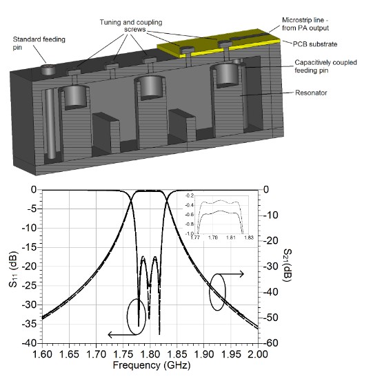
Fig. 1 Perspective view of cross section of designed 3-pole Chebyshev filter with novel feed structure (left) and Comparison of the simulated (dotted line) and measured (solid line) results. Inset shows the magnified view of the transmission coefficient (right)

[1] F. Pivit, S. Bulja and E. Doumanis, “A Radio Frequency Filter Comprising A Chamber, And A Method Of Filtering” , EU Patent, 818743, filed on April 2016.
Download here

Chia sẻ0
Tweet
Chia sẻ

Leave a Reply Cancel reply

Your email address will not be published. Required fields are marked *

Other Posts

Fig. 1 Perspective view of the structure of measurement LC cell

Characterisation and application of nematic liquid crystals in microwave devices

In-Vessel Resonant Communications

Performance Estimation of In-Vessel Resonant Communications

Profile & Bio

Senad Bulja, Ph.D., FIET, SMIEEE 

  1. Dr Bulja’s profile
  2. Email : contact@drbulja.com

PROFESSIONAL Profile

  • Accomplished career of over 19 years demonstrating consistent success as a Researcher, Leader and Mentor in the Wireless industry research environment.
  • Excellent Scientific contributions in the field of RF, EMC and telecommunications with 4 Nature Journal publications and over 70 peer-reviewed articles and conference papers
  • Strong leadership skills demonstrated by leading Ph.D. level educated cross-continental and cross-departmental teams to successful project execution.  
  • Proven Strategic Business Impact – introduced own developed technology into Nokia’s future technology roadmap (RF filters) and business transfer of the smart surface technology. 
  • Creative, internationally awarded and well-driven inventor with over 70 filed patents in the area of hardware for Radio Frequency (RF), Wireless Sensor Networks (WSN), Internet of Things (IoT) and wireless systems architectures. E.g. Nokia patent award entitled: “A top inventor in implementation patent first filings”, 2020.
  • Significant contribution in the identification of high revenue IP assets and leadership on the creation of Nokia’s patent portfolio roadmap. 
 

© Copyright 2023 drbulja.com. All Rights reserved