Variable attenuators, along with phase shifters, antennas and filters, are important RF devices widely used in modern telecommunication systems, such as in radar systems, point-to-point radio, smart antennas and Radio Frequency (RF) signal cancellation, to name a few. There exists a wide variety of attenuator types, depending on their architecture and implementation, however, one particular attenuator type has been dominant in the field of telecommunications. The Reflection-Type Attenuator (RTA) is a compact device and has been the mainstay in the telecommunications industry due to its compactness, low implementation cost, high dynamic range, and relatively low losses.
In the next sections, the principles of operation of RTAs are explained, however, it should be borne in mind that there exist many similarities with the design of RTPSs, as elaborated in depth in the previous article, entitled, “How to design a phase shifter?”.
RTA design
This section covers an in-depth design of RTA and is divided into two sections – RTA design with a single active device (such as PIN diode or cold FET) per reflective load and RTA design with multiple active devices per load. The section on RTA design with a single active device per reflective load covers the basics of RTA design, whereas the following section on RTA design with multiple active devices per reflective load presents more advanced techniques for increasing obtainable dynamic range.
RTA design with a single active device per reflective load
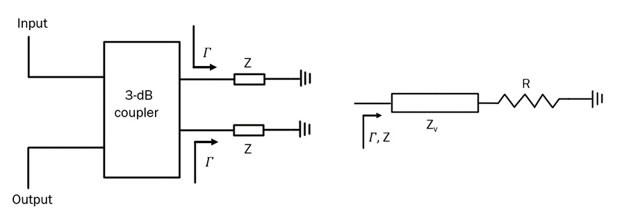
A generic circuit of an RTA based on a 3-dB coupler is shown in Fig.1. Under the assumption of an ideal 3-dB coupler and identical loads, Z = Zv + R, the expressions for the reflection and transmission coefficients of the RTA in Fig.1 can be written as [1, 2]:
(1) ![]()
where 𝛤 is the reflection at the loads, given by:
(2) ![]()
Just like in the case of RTPS, the structure of Fig.1 is inherently impedance matched and the reflection coefficient of the reflective loads becomes the transmission coefficient of the overall structure, i.e.
(3) ![]()
The magnitude of (3) can be written as:
(4) 
In other words, the amount of signal emanating from the output port is proportional to the value of impedance Zv. If this impedance is made variable, with imag(Zv) = 0, (4) simplifies to:
(5) ![]()
If the value of the termination resistor R is made to be equal to Z0, i.e. R = Z0, and impedance Zv is purely real and variable from very low values (ideally 0 Ω) to very high values (ideally infinite), the attenuator of Fig.1 can provide an infinitely high dynamic ratio. In other words, it is capable of fully passing the RF signal through without any attenuation, when the real value of variable impedance Zv is infinite and fully attenuating the RF signal for the case when the real value of variable impedance Zv is 0.
As with any RF components, this is never the case in practice. For example, the 3-dB coupler has a non-zero loss, typically, around 0.5 dB, while the variable impedance device, Zv, is limited by the both the lowest and highest resistances it can acquire, hence dictating the dynamic range of the RTA. For the purpose of the variable impedance device, at RF one usually uses a PIN diode (current-controlled device) or a “cold” FET (voltage-controlled device), however other possibilities exist [3]. The choice of the active device is dictated by several factors, such as the ON resistance, OFF capacitance, package parasitics and Inter-Modulation (IM) performance, to name but a few.
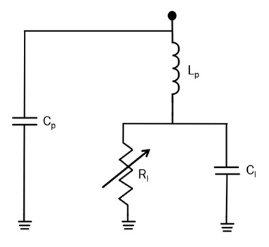
As an example, let us have a look at the PIN diode. An important parameter for PIN diodes is the carrier/recombination lifetime, which determines the lower frequency of operation. Below this frequency the PIN diode behaves as a standard PN diode, whereas above this frequency the PIN diode behaves as an almost current controlled resistor [4]. The carrier lifetime of the most commercially available PIN is usually from 5 ns to 5 μs, inferring the critical frequencies of 32 MHz and 32 kHz, respectively. Above these frequencies, the PIN diode behaves like a resistor. The high frequency equivalent circuit of a PIN diode is shown in Fig.2. The extrinsic parameters of the diode, Cp, and Lp stand for the package capacitance and package inductance, respectively. The values of the extrinsic parameters are greatly reduced through improvements of package quality, which, in turn, improves the parameters of the diode, however, these usually come at a monetary cost. For plastic packages, the values of Cp are usually in the range from 0.25 pF to 1 pF, whereas Lp depends on the length of the leads and can usually be assumed to be lower than 1 nH, unless otherwise stated in a datasheet. RI stands for the junction resistance and is inversely proportional to forward diode current, Idc:
(6) ![]()
Where, n, k and T stand for the diode coefficient, Boltzmann constant ![]() and absolute temperature, respectively. CI is the capacitance of the geometry dependent, intrinsic region of the diode, usually well below 1 pF. As can be seen, the PIN diode does not behave as an ideal variable resistor; instead, it contains a reactive part, which, in the circuit of the attenuator, depicted in Fig.1, limits the achievable dynamic range. A typical dynamic range of an RTA is, of course, dependent on the type diodes used and, but is usually in the range between 15 dB – 30 dB, with insertion losses being the range between 1 dB – 2 dB [5]. The bandwidth of operation of RTAs is limited by the bandwidth of the 3-dB couplers, which have traditionally experienced narrow percentage bandwidths, approximately 25%-30% when implemented in standard branch-line configurations. However, their bandwidth can be significantly increased by using impedance broad-banding techniques.
and absolute temperature, respectively. CI is the capacitance of the geometry dependent, intrinsic region of the diode, usually well below 1 pF. As can be seen, the PIN diode does not behave as an ideal variable resistor; instead, it contains a reactive part, which, in the circuit of the attenuator, depicted in Fig.1, limits the achievable dynamic range. A typical dynamic range of an RTA is, of course, dependent on the type diodes used and, but is usually in the range between 15 dB – 30 dB, with insertion losses being the range between 1 dB – 2 dB [5]. The bandwidth of operation of RTAs is limited by the bandwidth of the 3-dB couplers, which have traditionally experienced narrow percentage bandwidths, approximately 25%-30% when implemented in standard branch-line configurations. However, their bandwidth can be significantly increased by using impedance broad-banding techniques.
A question can now be asked if greater levels of dynamic range can be obtained than those presented using the structure in Fig.1? The answer is yes, and use will be made of the techniques already
elaborated in our previous article, entitled, “How to design a phase shifter?”. The next section addresses this point comprehensively.
RTA design with multiple varactor diodes per reflective load
The increase in the dynamic range in RTA with a single 3-dB coupler can be achieved in two ways – using either distributed circuits or lumped elements. RTA design using distributed circuits is described first.
RTA design with multiple varactor diodes per reflective load using distributed circuits
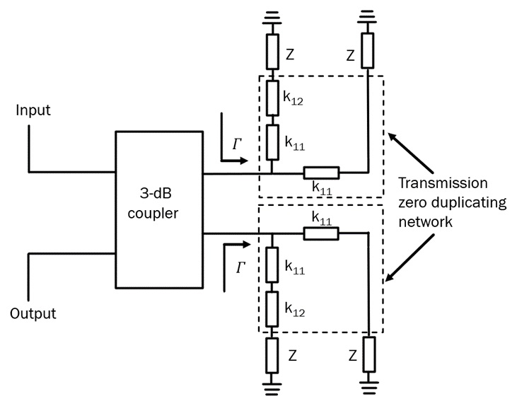
The generic RTA capable of doubling dynamic range provided by a single RTA as shown in Fig.1, is shown in Fig.3. Here, variable impedance Z, Z = Zv + R , as before represents a series connection of an active device (PIN diode, cold FET, etc) and a termination resistor, R, whose value is usually set to R = Z0. The condition for doubling the transmission zero is, as in the case with phase shifters, obtained by finding a double zero of the transmission coefficient obtained this way. The transmission coefficient of this circuit can be written as:
(7) ![]()
Here, k11 and k12 stand for quarter-wave (λ⁄4) transformers. For the circuit of Fig.3 represented by (7) to yield two times the dynamic range provided by the RTA of Fig.1, the transmission coefficient of (7) needs to be representable in the following form:
(8) ![]()
This is achieved by setting (7) to zero and solving it for Z:
(9) ![]()
The double zero condition is achieved when the discriminant in (9) is zero, which takes place when:
(10) ![]()
Inferring that the double zero of (7) occurs at:
(11) ![]()
Equating (11) to Z0, as required by (8), one obtains the value for k11:
(12) ![]()
Which upon substitution in (10), yields the value for k12:
(13) ![]()
According to (8), if conditions (12) and (13) are satisfied, the circuit of Fig.3 will deliver two times greater dynamic range. Expressions (12) and (13) infers that the conditions are satisfied only when the variable impedance device is purely real and attains low values, since, usually, but not always Z0 = 50Ω.
It is now possible to generalize the RTA shown in Fig.3 by recognizing that its reflective load plays a vital role in “doubling” the number of transmission zeroes and, hence, the achievable phase shift. By successively substituting variable impedance Z with the reflective load in Fig.3, it becomes possible to increase the dynamic range by n times, where n stands for the number of variable impedance Z circuits. Mathematically, the transmission coefficient in that case becomes:
(14) ![]()
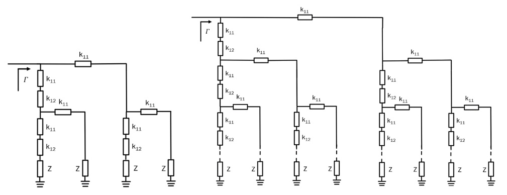
An example of the circuits containing 4 and an arbitrary number of reflective loads is shown in Fig.3. It is important to note that n cannot attain any integer number, but it is obtained in the following fashion: n = 2m, where m stands for the order of the RTA obtained in this way. For example, m = 0, n = 1, corresponds to the case with a single variable impedance Z, depicted in Fig.4 (left). The case with m = 1 and, hence, n = 2, corresponds to the case of Fig.3. The cases for m = 2, n = 4 and the general case of an arbitrary values of m and n, correspond to the reflective loads depicted in Fig.4.
Even though increase in dynamic ratio is enabled by the increase of the number of variable impedance Z sections, it is not possible to increase this number indefinitely. First, this is since circuits with a large number n can be impractical and, second, the addition of a large number of impedance transformers k11 and k12 lead to bandwidth reduction. For practical purposes, it is not recommended to have more than 4
variable impedance Z sections. A question could be posed now if, instead of the increased complexity of the reflective loads, the same result can be achieved using a simple replication of the RTAs shown in Fig.1. The answer to this question will entirely depend on the losses exhibited by these two RTA types.
The general expression the losses of a cascade connection of n number of single variable impedance Z RTAs can be expressed as:
(15) 
whereas the losses of the RTA with the generalized transmission zero duplicating reflective loads as shown in Fig.4 (right) can be expressed as:
(16) 
In (15) and (16), Lcoupler, stand for RF losses in the 3-dB coupler, Lint.conn.line stands for the losses of the microstrip lines connecting n single variable impedance RTAs, Lbias.circuit stands for the losses in the dc bias network and Ldupl.zero.network.dist stands for the losses of the distributed “duplicating” network, as shown in dashed line in Fig.4 (right). The difference between (15) and (16) is:
(17) ![]()
This equation shows that the difference in the losses of (15) and (16) is dependent on the losses of the 3-dB couplers, interconnecting lines, losses in the DC biasing circuit and the losses of the transmission zero duplicating network. This implies that the benefits gained using the reflective load replicating circuits as generally shown in Fig.4 (right) will be fully dependent on the exact realization of the RTA.
RTA design with multiple varactor diodes per reflective load using lumped elements
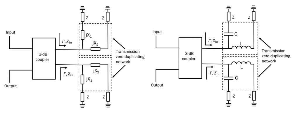
The generic RTA capable of doubling the dynamic ratio provided by an RTA terminated in reflective loads containing variable impedance Z as shown in Fig.1 using lumped elements is shown in Fig.5 (left). Just like in the case with phase shifters, the condition to double the dynamic range is reached when:
(18) ![]()
Using this condition, the reflection coefficient of the circuit of Fig.5 (left) becomes:
(19) ![]()
Just like in the previous case with distributed elements, the required condition for the doubling of dynamic range is achieved when (19) can be expressed as:
(20) ![]()
This is achieved by finding the roots of (19) i.e.:
(21) ![]()
The necessary condition for the achievement of double zero of (20) is that the discriminant of (21) is zero, which yields:
(22) ![]()
Which upon substitution into (21) provides:
(23) ![]()
Combining (18), (22) and (23) finally provides:
(24) ![]()
In other words, the lumped elements X_1 and X_2 are reactances of identical magnitudes, but of opposite signs – one is an inductor, and the other one is a capacitor. If we assume that X_1 is a capacitor and X_2 is an inductor, their exact values are calculated from:
(25) ![]()
Where ω stands for the angular frequency of operation. Just like in the case using distributed elements,
here, too, is also possible to generalize the RTA shown in Fig.4 for an arbitrary order of the reflective load network. Fig.6 (left) depicts the case when the reflective loads are terminated in 4 variable impedances, Z, and Fig.6 (right) depicts the general case when the reflective loads are terminated in an arbitrary number of variable impedances. In a similar manner as with distributed reflective loads in the previous section, it is instructive to compare the losses exhibited by the proposed RTA structure and the losses obtained by a cascade connection of n number of single variable impedance Z RTAs, given by (15).

The losses exhibited by the cascade connection of the proposed reflective loads can be written as:
(26) 
The difference between the losses given by (15) and (26) can now be written as:
(27) ![]()
Just like in the previous case with the transmission zero “duplicating” network realized in the distributed form the difference of the losses given by (15) and (26) is dependent on the losses of the 3-dB couplers, interconnecting lines, losses in the DC biasing circuit and the losses of the lumped element transmission zero duplicating network. Since in the present case the transmission zero “duplicating” network is composed of lumped elements – one inductor and one capacitor, its losses are expected to be lower than the losses of the interconnecting lines, however, this is entirely dependent on the exact RTA realization. It would now be instructive to design an RTA and demonstrate achievable dynamic ranges. This is provided in the next section.
Example – RTA design
Let us design several RTAs using the theory in the previous sections operating at a centre frequency of f0 = 2.5 GHz . As the active device, assume a PIN diode from Skyworks [6] with a parasitic capacitance of Cp = 0.35 pF and parasitic inductance of Lp = 1 nH. The minimum series resistance of the diodes is 0.5 Ω. Assume all other components to be lossless.
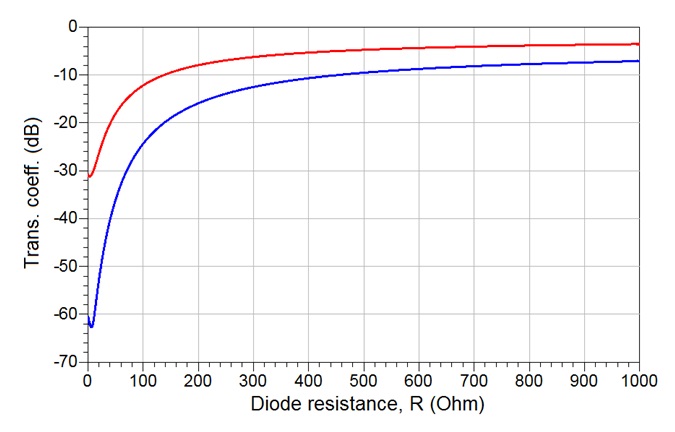
Solution: The PIN diode of [6] achieves the variation of its resistance from 1000 Ω (zero current) to 0.5 Ω (100 mA current). Using this PIN diode in series with a 50 Ω resistor in the reflective load, as shown in Fig.1, one achieves the variation of attenuation as indicated in Fig.7. The results are obtained using Keysight’s Advanced Design System (ADS), [7]. As evident from this figure, the maximum attenuation is achieved when the PIN diode is fully ON, i.e. when its resistance is around 0.5 Ω to yield the attenuation of 15.5 dB. As the current through the PIN diode is reduced, (or its resistance increased), the power dissipated on the termination resistor reduces and more power is passed to the output. At a diode resistance of approximately 1000 Ω, the insertion loss becomes 1.8 dB. This infers that the dynamic range of the attenuator obtained in this is around 13.7 dB. As a next step, the RTA circuits enabling doubling and quadrupling of dynamic range using distributed, Fig.4, elements. In this case, considering Z0 = 50 Ω, the impedance transformers k11 and k12 from (12) and (13), respectively, become ![]() and k12 = 50Ω. The attenuation as function of the diode resistance of the RTAs designed in this way are presented in Fig.8. As can be seen, the values of attenuation have increased correspondingly. Such circuits have increased the dynamic range in proportion to the number of PIN
and k12 = 50Ω. The attenuation as function of the diode resistance of the RTAs designed in this way are presented in Fig.8. As can be seen, the values of attenuation have increased correspondingly. Such circuits have increased the dynamic range in proportion to the number of PIN
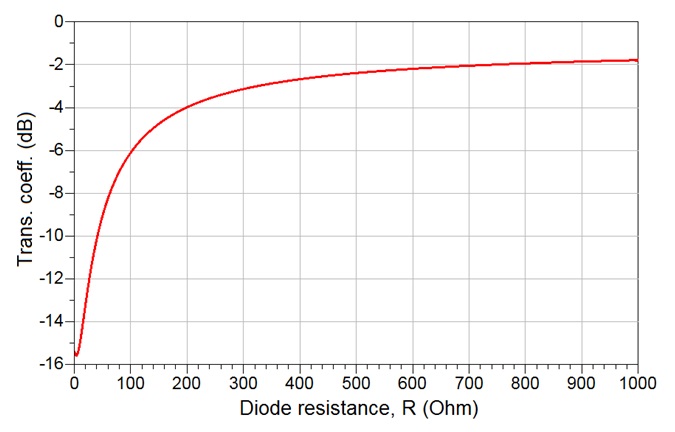
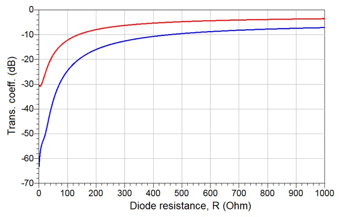
diodes – 27.6 dB for the 2 PIN diode per load RTA and 55.5 dB for the 4 PIN diode RTA per load. In a similar manner, the values of the lumped element RTAs, L and C are calculated using (25) to yield C = 1.27 pF and L = 3.18 nH. The attenuation as a function of the diode resistance of the RTAs designed in this way is presented in Fig.9. Just like in the case depicted in Fig.8, the dynamic range has increased – in the case of the 2 PIN diode lumped element RTA the dynamic range is now 27.2 dB, while for the 4 PIN diode counterpart it stands at 55.9 dB, which are in line with the dynamic range values obtained for their distributed element counterparts.
In practice, the exact values of attenuation will be ultimately dependent on the exact realizations of such circuits. For example, the losses in the 3-dB coupler, PIN diode, lumped and distributed elements and PCB substrate will all influence the extent of achieved phase shift and, ultimately, the losses. The choice of the attenuator will, therefore, be entirely dependent on the application and frequency of operation and, in many cases, the real estate available on PCB board.
Conclusion
In this article a comprehensive study on how to design Reflective Type Attenuators (RTAs) is presented. The article concludes with an example demonstrating agreement between the developed theory and simulations.
References
[1] S. Bulja, A. Grebennikov and P. Rulikowski, “Theory, analysis and design of high order reflective, absorptive filters,” in IET Microwaves, Antennas and Propagation, vol. 11, issue 6, pp.787-795, 2017.
[2] V. Kirillov, D. Kozlov and S. Bulja, “Series vs Parallel Reflection-type Phase Shifters”, IEEE Access, vol. 8, Oct. 2020, doi:10.1109/ACCESS.2020.3030463.
[3] S. Bulja and A. Grebennikov, “Variable Reflection-Type Attenuators Based on Varactor Diodes”, IEEE Trans. Microwave Theory and Tech., vol. 60, issue 12, 3719-3727, 2012.
[4] https://www.qsl.net/n9zia/an922.pdf
[5] https://www.skyworksinc.com/-/media/SkyWorks/Documents/Products/2001-2100/SKY12236_11_202529H.pdf
[6] https://www.skyworksinc.com/-/media/SkyWorks/Documents/Products/2201-2300/SMP1331_087LF_203589B.pdf
[7] https://www.keysight.com/us/en/products/software/pathwave-design-software/pathwave-advanced-design-system.html
Leave a Reply