Phase shifters, together with filters and antennas, form one of the basic building blocks of modern telecommunication systems. They are extensively used in radar, phased-arrays, receiver systems and many other types of communication networks. There exists a wide variety of phase shifter types, depending on their architecture and implementation, however, one particular phase shifter type has been dominant in the field of telecommunications. The Reflection-Type Phase Shifter (RTPS) is a compact device and has been the mainstay in the telecommunications industry due to its compactness, low implementation cost, high values of achievable phase shift and relatively low losses. Due to its importance to the telecommunications industry, it is pertinent to examine its history in more detail.
The first ever RTPS was proposed by Hardin in 1960 [1]. His experimental set-up, comprising of a circulator and a varactor diode, is shown in Fig. 1. The principle of operation is rather simple – the input signal at Port 1 is reflected by the reactance of the varactor diode at Port 2 and, by virtue of circulator operation, emerges from Port 3. The extent of phase shift is directly influenced by the capacitance ratio of the varactor diode and in the case of Fig. 1, it attains rather modest values. The use of a varactor diode resonated with an inductor, as a means to increase low values of phase shift was proposed by Searing in 1961 [2]. However, it was not until 1969, Garver, [3] when the first thorough treatment of RTPSs was provided. In that classical paper, Garver presented the conditions for achieving a 360o phase shift in a linear fashion. From this point in time, rapid development of phase shifting circuits followed. The bulky circulators were replaced with lightweight and cost-effective 3-dB couplers and a wide variety of reflective loads were investigated. These focused on either increasing the phase shift tuning range, bandwidth, power handing capability or miniaturisation – Terrio [4], Glance, [5], White, [6], Dawson, [7] and Chen, [8], Malczewski, [9]. Even to this day, RTPSs draw considerable attention. Due to this, in the next section, the exact operation of the RTPS will be explained, together with ways of increasing their phase shift range.
![Fig. 1 Circulator based RTPS – Hardin, 1960 [1]](https://drbulja.com/wp-content/uploads/2024/02/1-1.png)
RTPS design
This section covers an in-depth design of RTPS and is divided into two sections – RTPS design with a single active device (such as varactor diode) per reflective load and RTPS design with multiple varactor diodes per load. The section on RTPS design with a single varactor diode per reflective load covers the basics of
RTPS design and details how phase shift can be maximized. The following section on RTPS design with multiple varactor diodes per reflective load builds upon the previous section to present more advanced techniques for increasing obtainable values of phase shift.
RTPS design with a single varactor diode per reflective load
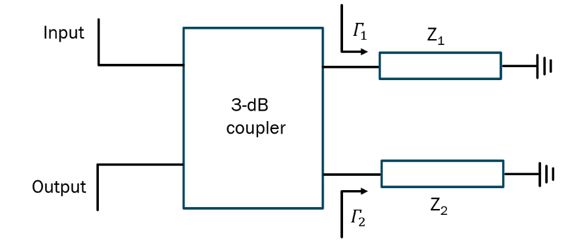
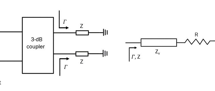
A generic circuit of an RTPS based on a 3-dB coupler is shown in Fig. 2.
Under the assumption of an ideal 3-dB coupler, the expressions for the reflection and transmission coefficients of the structure of Fig. 2 become [10, 11]:
S11=0.5*(Γ1-Γ2) and S21=-j*0.5*(Γ1-Γ2) (1)
If the reflective loads are the same, i.e.,Γ1=Γ2=Γ, implying that Z1=Z2=Z, (1) simplifies to S11=0 and S21=-j*Γ . In other words, the structure of Fig. 2 is inherently impedance matched and the reflection coefficient of the reflective loads becomes the transmission coefficient of the overall structure. 𝛤 is then equal to:
Γ=(Z-Z0)/(Z+Z0) (2)
Where Z0 is the characteristic impedance of the interconnecting line and Z is the impedance of reflective loads. The general expression for the phase component of (2) can be written as:

For the case when the reflective loads are composed of a varactor diode (or any other device capable of variable reactance) with a capacitance ratio r=Cmax/Cmin , the magnitude of the reflective coefficient at the loads and hence the overall structure becomes, inferring no losses, while the exact value of phase shift becomes:

Finding the first derivative of (4) reveals that its maximum occurs when to yield the maximum phase shift of 180o.
As mentioned in the previous section, phase shift can be increased by introducing an inductor in the circuit of the varactor diode. The inductor can be connected both in series and in parallel with some interesting implications with regards to the exact values of obtainable phase shift. Both configurations are shown in Fig. 3. The value for the inductor, as shown in Fig.3, needed for the maximum obtainable phase shift is found by obtaining the first derivative of:


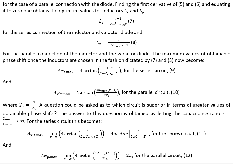
(12) indicates that the parallel connection as shown in Fig. 3 (right) can achieve a full 360o phase shift using only one varactor diode, whereas for the case of the series connection, the maximum achievable phase shift is a function of the characteristic impedance, frequency and the minimum diode capacitance. Also, such a circuit is not theoretically possible to achieve a full 360o phase shift unlike with the case of the parallel connection. An excellent examination of the series vs parallel reflective load configurations is presented in [11], which, in addition to examining the linear parameters (phase shift and insertion losses), also examines their non-linear characteristics. The article concludes that the parallel inductor-varactor combination is superior in every aspect to its series connection counterpart. However, in practice, the series inductor-varactor combination is more widely used – one of the possible reasons lies with the ease of DC biasing of the varactor diode in such a configuration. In this aspect and with reference to Fig. 3 (left), the application of DC bias on varactor diode can be done directly as the series inductor, , provides a short to the ground. One the other hand, the parallel combination requires addition of a decoupling capacitor in series with inductor , so that the applied DC bias voltage is not shorted through inductor .
A question can now be asked if phase shifts greater than those presented in this section are obtainable? The answer is yes, and the next section addresses this point comprehensively.
RTPS design with multiple varactor diodes per reflective load
The increase in the values of obtainable phase shift using an RTPS with a single 3-dB coupler can be achieved in two ways – using either distributed circuits or lumped elements. RTPS design using distributed circuits is described first.
RTPS design with multiple varactor diodes per reflective load using distributed circuits
The generic RTPS capable of doubling phase shift provided by an RTPS terminated in reflective loads containing variable impedance Z as shown in Fig. 4 (left) is shown in Fig. 4, (right). Here, variable impedance Z can take many forms – it could be a simple varactor diode or series/parallel connection or a varactor diode and an inductor. The transmission coefficient of this circuit (Fig. 4, right) can be written as:

Here, and stand for quarter-wave ((λ⁄4)) transformers. For the circuit of Fig. 4 (right) represented by (13) to yield two times the amount of phase shift provided by the RTPS of Fig. 4 (left), the transmission coefficient of (13) needs to be representable in the following form:

In other words, (14) depicts the situation that is equivalent to having two circuits of Fig. 4 (left) connected in series. Mathematically, the phase component of (14) now becomes:

To have (13) representable by (14) its two transmission zeroes need to be identical. This is achieved by setting (13) to zero and solving it for Z:
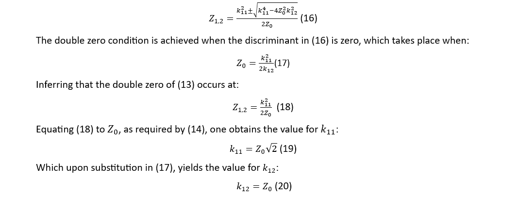
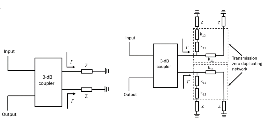
According to (14), if conditions (19) and (20) are satisfied, the circuit of Fig. 4 (right) will deliver two times greater phase shift than the one provided in Fig. 4 (left).
It is now possible to generalize the RTPS shown in Fig. 4 (right) by recognizing that its reflective load plays a vital role in “doubling” the number of transmission zeroes and, hence, the achievable phase shift. By successively substituting variable impedance Z with the reflective load in Fig. 4 (right), it becomes possible to increase obtainable phase shift by n times, where n stands for the number of variable impedance Z circuits. Mathematically, the transmission coefficient in that case becomes:

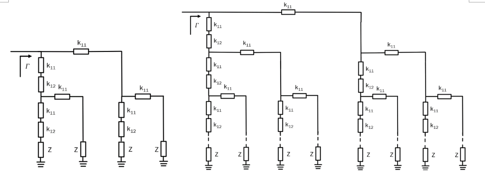
An example of the circuits containing 4 and an arbitrary number of reflective loads is shown in Fig. 5. It is important to note that n cannot attain any integer number, but it is obtained in the following fashion: n = 2m, where m stands for the order of the RTPS obtained in this way. For example, m = 0, n = 1, corresponds to the case with a single variable impedance Z, depicted in Fig. 4 (left). The case with m = 1 and, hence, n = 2, corresponds to the case of Fig. 4 (right). The cases for m = 2, n = 4 and the general case of an arbitrary values of m and n, correspond to the reflective loads depicted in Fig. 5.
Even though increase in phase shift is enabled by the increase of the number of variable impedance Z sections, it is not possible to increase this number indefinitely. First, this is since circuits with a large number n can be impractical and, second, the addition of a large number of impedance transformers and lead to bandwidth reduction. For practical purposes, it is not recommended to have more than 4 variable impedance Z sections.
A question could be posed now if, instead of the increased complexity of the reflective loads the same result can be achieved using by a simple replication of the RTPSs shown in Fig. 4 (left). The answer to this question will entirely depend on the losses exhibited by these two RTPS types.
The general expression the losses of a cascade connection of n number of single variable impedance Z RTPSs can be expressed as:

whereas the losses of the RTPS with the generalized transmission zero duplicating reflective loads as shown in Fig. 5 (right) can be expressed as:

In (22) and (23), Lcoupler, stand for RF losses in the 3-dB coupler, L(int_conn_line) stands for the losses of the microstrip lines connecting n single variable impedance RTPSs, L(bias_circuit) stands for the losses in the dc bias network and L(dupl_zero_network_dist) stands for the losses of the distributed “duplicating” network, as shown in dashed line in Fig. 4 (right). The difference between (22) and (23) is:
![]()
This equation shows that the difference in the losses of (22) and (23) is dependent on the losses of the 3-dB couplers, interconnecting lines, losses in the DC biasing circuit and the losses of the transmission zero duplicating network. This implies that the benefits gained using the reflective load replicating circuits as generally shown in Fig. 5 (right) will be fully dependent on the exact realization of the RTPS.
RTPS design with multiple varactor diodes per reflective load using lumped elements
The generic RTPS capable of doubling phase shift provided by an RTPS terminated in reflective loads containing variable impedance Z as shown in Fig. 4 (left) using lumped elements is shown in Fig. 6 (left). Just like in the previous section, variable impedance Z can take many forms – it could be a simple varactor diode or series/parallel connection or a varactor diode and an inductor. The input impedance of the reflective loads, as depicted in Fig. 6 (right) can be written as:

Just like in the previous case with distributed elements, the required condition for the doubling of phase shift is achieved when (27) can be expressed as:
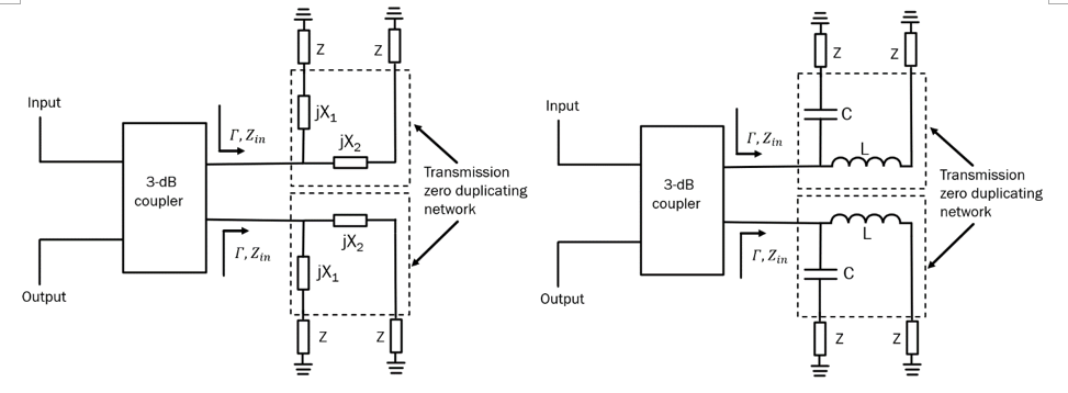
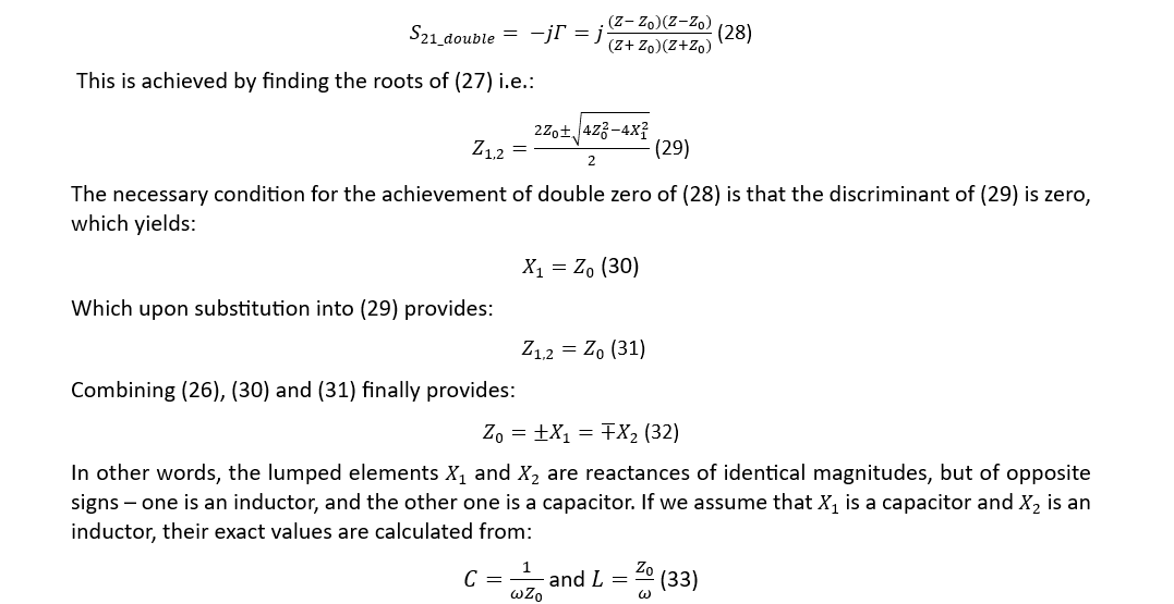
Where ω stands for the angular frequency of operation. Just like in the case using distributed elements, here, too, is also possible to generalize the RTPS shown in Fig. 6 for an arbitrary order of the reflective load network. Fig. 7 (left) depicts the case when the reflective loads are terminated in 4 variable impedances, Z, and Fig. 7 (right) depicts the general case when the reflective loads are terminated in an arbitrary number of variable impedances.
In a similar manner as with distributed reflective loads in the previous section, it is instructive to compare the losses exhibited by the proposed RTPS structure and the losses obtained by a cascade connection of n number of single variable impedance Z RTPs, given by (22). The losses exhibited by the cascade connection of the proposed reflective loads can be written as:


The difference between the losses given by (22) and (34) can now be written as:
![]()
Just like in the previous case with the transmission zero “duplicating” network realized in the distributed form the difference of the losses given by (22) and (35) is dependent on the losses of the 3-dB couplers, interconnecting lines, losses in the DC biasing circuit and the losses of the lumped element transmission zero duplicating network. Since in the present case the transmission zero “duplicating” network is composed of lumped elements – one inductor and one capacitor, its losses are expected to be lower than the losses of the interconnecting lines, however, this is entirely dependent on the exact RTPS realization. It would now be instructive to design an RTPS and demonstrate achievable phase shifts. This is provided in the next section.
Example – RTPS design
Let us design several RTPSs using the theory in the previous sections operating at a centre frequency of f0=2.5 GHz . As the active device, assume a varactor diode with a minimum capacitance of Cmin=1 pF and capacitance ratio of r=5. The parasitic resistance of the diode is 1 Ω. Assume all other components to be lossless.
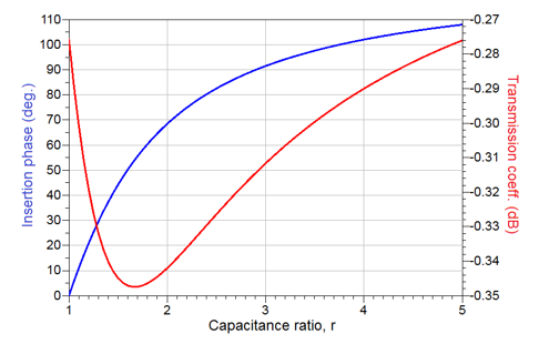
Solution: Let assume that the basic variable impedance will be a series configuration of a varactor diode and an inductor, as shown in Fig. 3 (left). For the given parameters of the varactor diode, the value of the series inductor, Ls, is calculated using (7) to yield Ls = 2.53 nH. In conjunction with (9), this value yields the maximum, theoretically achievable phase shift of 107.9o, obtained using Keysight’s Advanced Design System (ADS), [12]. The phase and magnitude of the transmission coefficient as a function of capacitance ratio r are shown in Fig. 8. As evident, the obtained phase shift is in full alignment with predictions.
As a next step and based on the optimal series reflective load comprising the series inductor, Ls = 2.43 nH, the RTPS circuits enabling doubling of the amount of phase shift using distributed, Fig. 4 (right), and lumped elements, Fig. 6 (right), are designed.
For the distributed element circuit and considering Z0 = 50 Ω, the impedance transformers and from (19) and (20), respectively, become and . In a similar manner, the values of the lumped elements, L and C are calculated using (34) to yield and . The insertion phase and loss as function of capacitance ratio, r, of the RTPS designed in this way are presented
in Fig. 9. As can be seen, the values of insertion phase and transmission loss are identical in both cases, and both have resulted in doubling of the achievable phase shift, at the expense of doubling the insertion losses, as predicted. The maximum achieved phase shift achieved in this case is 215o. This is the direct consequence of the fact that no losses are assumed for both the distributed and lumped elements of the RTPS circuits.
Lastly, the response of the RTPS realized using 4 optimal variable impedance loads in both the distributed, Fig. 5 (left), and lumped, Fig. 7 (left). The responses of such circuits are shown in Fig. 10. As predicted, the
insertion phase is now 4 times greater than the insertion phase of a single load RTPS and it stands, for both distributed and lumped element realizations, at 432o. Also, the insertion loss has also increased 4-fold compared to the single load RTPS realization.
However, the exact values of phase shift and losses of RTPSs will be ultimately dependent on the exact realizations of such circuits. For example, the losses in the 3-dB coupler, varactor diode, lumped and distributed elements and PCB substrate will all influence the extent of achieved phase shift and, ultimately, the losses. The choice of the phase shifter will, therefore, be entirely dependent on the application and frequency of operation and, in many cases, the real estate available on PCB board.
Conclusion
In this article a comprehensive study on how to design Reflective Type Phase Shifters (RTPS) is presented. The study was initiated with a brief history of RTPS and basic principles in order to explain the maximum, theoretical values of achievable phase shifts that can be expected using simple varactor diode circuits. The study then proceeded to systematically present ways of increasing the amount of phase shift by modifying reflective load circuits. The article concludes with an example demonstrating agreement between the developed theory and simulations.


References:
[1] R. N. Hardin, E. J. Downey and J. Munushian, ‘Electronically variable phase shifter utilizing variable capacitance diodes’, Proc. IRE, vol. 48, pp. 944-945, May 1960.
[2] R. M. Searing, ‘Variable capacitance diodes used as phase-shift devices’, Proc. IRE, vol. 49, pp. 640-641, March 1961.
[3] R. V. Garver, ‘360o Varactor linear phase modulator’, IEEE Trans. Microwave Theory Tech., vol. MTT-17, no. 3, pp. 137-147, March 1969.
[4] F. G. Terrio, R. J. Stockton and W. D. Sato, ‘A low-cost P-I-N diode phase shifter for airborne phased-array antennas’, IEEE Trans. Microwave Theory and Tech., vol. MTT-22, no. 6, pp. 688-692, June 1974.
[5] B. Glance, ‘A fast low-loss microstrip p-i-n phase shifter’, IEEE Trans. Microwave Theory and Tech., vol. MTT-27, no.1, pp. 14-16, January 1979.
[6] J. F. White, ‘Diode phase shifters for array antennas’, IEEE Trans. Microwave Theory and Tech., vol. MTT-22, no. 6, pp. 658-674, June 1974.
[7] D. E. Dawson et al., ‘An analog X-band phase shifter’, IEEE MTT-S Int. Microwave Symp. Dig., pp. 6-10, 1984.
[8] C. L. Chen et al., ‘A low loss Ku-band monolithic analog phase shifter’, IEEE Trans. Microwave Theory Tech., vol. MTT-35, no.3., pp. 315-320, March 1987.
[9] A. Malczewski et al., ‘X-band RF MEMS phase shifters for phased array applications’, IEEE Microwave and Guided Letters, vol. 9, no. 12, pp. 517-519, December 1999.
[10] S. Bulja, A. Grebennikov and P. Rulikowski, “Theory, analysis and design of high order reflective, absorptive filters,” in IET Microwaves, Antennas and Propagation, vol. 11, issue 6, pp.787-795, 2017.
[11] V. Kirillov, D. Kozlov and S. Bulja, “Series vs Parallel Reflection-type Phase Shifters”, IEEE Access, vol. 8, Oct. 2020, doi:10.1109/ACCESS.2020.3030463.
Leave a Reply