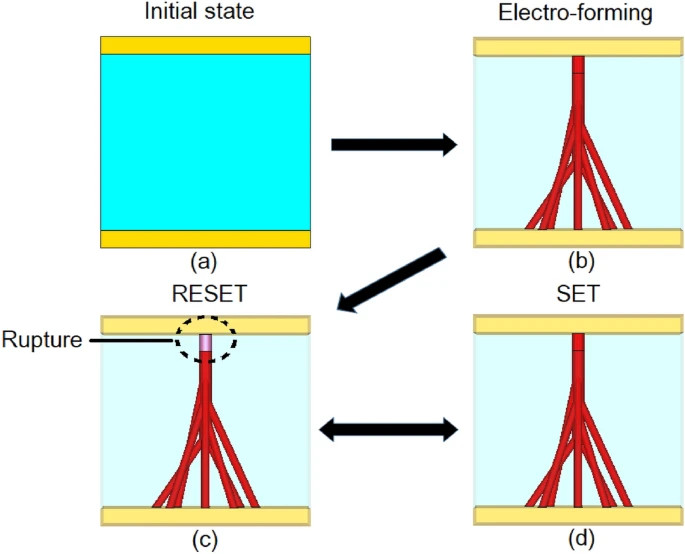
Resistive switching (RS) of Transition Metal Oxides (TMOs) has become not only an attractive choice for the development of next generation non-volatile memory, but also as a suitable family of materials capable of supporting high-frequency and high-speed switching needed for the next generation wireless communication technologies, such as 6G. The exact mechanism of RS is not yet clearly understood; however, it is widely accepted to be related to the formation and rupture of sub-stoichiometric conductive filaments (Magnéli phases) of the respective oxides upon activation, as shown in Fig. 1.

Fig. 1: Formation and rupture of conductive filaments (electroforming); (a) initial state, (b) electro-formation of filament, (c) rupture of filament, RESET state and (d) reversible SET state
The physical mechanism behind Resistive Switching (RS) based on Transition Metal Oxides (TMOs) relies on the reversible transition from the dielectric to conductive states, commonly referred to as Mott transition. The metal-insulator transition in VO2 (TMO) is now accepted to be a (homogeneous) bulk phenomenon, however, the working of RS of the remaining TMOs can be attributed to the formation and rupture of conductive filaments, Fig. 1, in the interior of the material upon the application of DC bias voltage or temperature elevation. To this end, the filamentary conduction mechanism was experimentally confirmed through in-situ measurements of currents and voltages in TinO2n-1 and NiO.
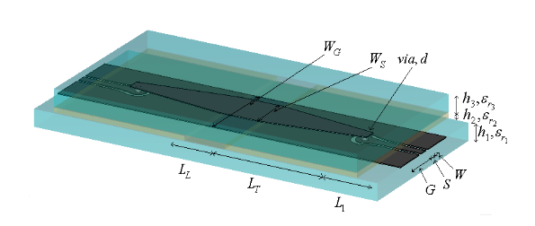
The use of TMOs in mm-wave applications has been largely limited to the crystalline oxides of vanadium (VOx), which leaves a large knowledge and applications gap with regards to the behaviour and possible use of other TMOs for mm-wave frequencies. In this paper, we examine the switching behaviour of amorphous TiO2 and NiO both under the DC regime and in the high frequency mode. We show that the DC resistance of amorphous TiO2 is invariant of the length of the active region. In contrast, the resistance of the NiO samples exhibits a strong dependence on the length, and its DC resistance reduces as the length is increased. We further show that the high frequency switching characteristics of TiO2, reflected in insertion losses in the ON state and isolation in the OFF state, are far superior to those of NiO. Fundamental inferences stem from these findings, which not only enrich our understanding of the mechanism of conduction in binary/multinary oxides but are essential for the enablement of widespread use of binary/multinary oxides in emerging non-volatile memory and 6G mm-wave applications. As an example of a possible application supported by TMOs, is a Reflective-Type Variable Attenuator (RTVA), shown here. It is designed to operate at a centre frequency of 15 GHz. The results indicate that it has a dynamic range of no less than 18dB with a maximum insertion loss of 2.1dB.
Conclusions
The versatile nature of TMOs and in the present case TiO2 strongly requires further investigation. Our results on the switching characteristics of TiO2 show that a TMO does not the need to be in a “perfect” crystalline state in order to exhibit good RF/mm-wave switching characteristics, rather they point to the fact that even amorphous TMOs can display attractive RF/mm- wave characteristics. A major research question to answer lies with the possibility of tailoring the RF/mm-wave switching characteristics of amorphous TMOs by virtue of controlling the level of “defects” or impurities. This will be an exciting time for TMO research as the levels of reconfigurability achieved so far are extremely promising and further research work is necessary to fully unlock their potential.


Leave a Reply