Dr. Senad Bulja, PhD, FIET, SMIEEE

  • Home
  • Researches
  • Workshops
  • Patents
  • Products
  • Tutorials
  • Solutions
  • Services

Researches

Home » Researches » Complex dielectric permittivity extraction based on multilayer thin film microstrip lines

Complex dielectric permittivity extraction based on multilayer thin film microstrip lines

Dr. Senad Bulja 21/12/2022Download PDF

In this paper/study we report on an analytical method to extract complex relative dielectric permittivities of multi-layered dielectric substrates used to construct Thin-Film (thicknesses below skin depth) Microstrip Line (TFML) structures. Electrically thin conductors, due to their finite conductivity, exhibit extraordinary conductor and radiation losses, with a dispersion relationship non-consistent with standard, thick conductors. In essence, thin conductors exhibit a slow-wave behavior, similar to high k dielectrics. In this aspect, separating the contributions of the thin conductors and dielectric substrates on wave propagation on TFML is a challenging task at best. Several attempts have been to address this difficult task, however with very little success.

In combination with the unknown dielectric parameters of substrates, the problem appears impossible to solve. However, by employing mapping techniques and transforming the problem of unknown dielectric parameters of a TFML to a problem of unknown dielectric parameters of a Parallel-Plate Wave-Guide (PPWG), we were able to separate the contributions of the thin conductors and dielectric substrates on wave propagation. Our analysis and measurements indicate that the accuracy of the proposed technique is between 5% (wide TFML, W/H = 80) and 15% (narrow TFML, W/H = 5).

The results are of tremendous importance to the already deploying 5G systems and forthcoming 6G systems, both of which stipulate the use of high frequencies (FR2 – 28&39 GHz for 5G), while even higher frequencies are predicted for 6G. The primary reason for this lies with the trend towards the usage of thin conductors as telecommunications hardware (such as filters and antenna) becomes smaller as frequency increases. Therefore, taking into account the effect of thin conductors is mandatory as frequency increases.


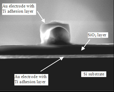
Fig. 1 Cross section of TFML

Chia sẻ0
Tweet
Chia sẻ

Leave a Reply Cancel reply

Your email address will not be published. Required fields are marked *

Other Posts

Fig. 1 Perspective view of the structure of measurement LC cell

Characterisation and application of nematic liquid crystals in microwave devices

In-Vessel Resonant Communications

Performance Estimation of In-Vessel Resonant Communications

Profile & Bio

Senad Bulja, Ph.D., FIET, SMIEEE 

  1. Dr Bulja’s profile
  2. Email : contact@drbulja.com

PROFESSIONAL Profile

  • Accomplished career of over 19 years demonstrating consistent success as a Researcher, Leader and Mentor in the Wireless industry research environment.
  • Excellent Scientific contributions in the field of RF, EMC and telecommunications with 4 Nature Journal publications and over 70 peer-reviewed articles and conference papers
  • Strong leadership skills demonstrated by leading Ph.D. level educated cross-continental and cross-departmental teams to successful project execution.  
  • Proven Strategic Business Impact – introduced own developed technology into Nokia’s future technology roadmap (RF filters) and business transfer of the smart surface technology. 
  • Creative, internationally awarded and well-driven inventor with over 70 filed patents in the area of hardware for Radio Frequency (RF), Wireless Sensor Networks (WSN), Internet of Things (IoT) and wireless systems architectures. E.g. Nokia patent award entitled: “A top inventor in implementation patent first filings”, 2020.
  • Significant contribution in the identification of high revenue IP assets and leadership on the creation of Nokia’s patent portfolio roadmap. 
 

© Copyright 2023 drbulja.com. All Rights reserved