
Microstrip antennas have been extensively used in the past because of their several advantages (low weight, low cost, conformability and low profile) over conventional antennas. However, their small impedance bandwidth has always been a major constraint as it limits the frequency range over which the antenna can perform satisfactorily. As many authors have shown it, employing thick dielectrics can increase the bandwidth, but at the expense of reduction of the cut-off frequency of surface waves and as a result, the distortion of the radiation pattern. Furthermore, in many applications, a high profile microstrip antenna is not desirable.
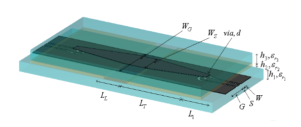
Broadbanding using stacked configurations was first introduced by Sabban [1], where the feeding and the radiating patch were separated by an air region. The work in [1] is then further extended in [2], where for different values of the air region, the bandwidths and the radiation patterns are examined. In this paper, a broadbanding concept using unequal patch sizes and without an air region separation is proposed and applied to double and triple patch antennas. In order to show the development of the concept, initially, the single and the double patch microstrip antenna developed on low profile substrates with the same overall thickness and dielectric constant, are studied. Then the development of the low-profile triple patch antenna on three substrates with the same overall thickness as those of the single and double patch microstrip antenna is reported. The physical appearance of the triple patch antenna is presented in Fig. 1. It is fed by a microstrip line connected to the middle patch.
The proposed antenna has a thickness of 3.06 mm and was developed to provide a bandwidth of 22 % about the centre frequency of 5 GHz. Here, the feed line had to be applied to the middle patch. Although not reported in this paper, it was found that the antenna is scalable for operation at other centre frequencies.
 and reflection coefficient for the proposed triple patch antenna (right): (a) simulated and (b) measured")
[1] Sabban, A: “A new broadband stacked two-layer microstrip elements “, Electronic Letters, 1983, pp. 63-66.
[2] Lee, R.Q., “Characteristics of a two – layer electromagnetically coupled rectangular patch antenna”, Electronic Letters, 1987, Vol. 23, pp.1070 – 1072.
Leave a Reply