Radio Frequency (RF) filters are very important in all types of telecommunications equipment. They help filter out the unwanted frequencies and only let the frequencies that the communication system is designed for pass through. They are used both in Time Division Duplex (TDD) and Frequency Division Duplex (FDD) systems, however there are some slight differences between them. For example, filters in FDD systems usually need to meet stricter electrical requirements compared to their TDD counterparts – this is simply since in FDD systems the transmit (TX) and receive (RX) channels are frequency separated whereas in TDD systems they occupy the same frequency band but operate at interleaved time intervals. As such, in FDD systems, filters need to be carefully designed to avoid signal leakage between its TX and RX branches. Usually, the leakage from TX to RX is of greater concern due to much higher powers involved with the TX channel. Such problems do not exist with TDD systems as the entire filter’s passband is shared between the TX and RX channels.
Depending on the type of telecommunications system and its filtering requirements, filters come in a variety of flavours. Examples include cavity filters, ceramic filters and Printed Circuit Board (PCB) filters, to name but a few. The choice of the filter for a particular application depends on the electrical and space requirements. Usually, the highest performing filters are ceramic based with Quality (Q) factors of individual resonators up to 5,000. They are closely followed by silver-plated metal cavity filters with individual resonator Q-factors of up to 3,000-3,500. PCB resonators are among the lowest performing resonators with individual resonator Q-factors rarely exceeding 200-300, however, this is strongly dependent on the losses of the PCB substrate.
Any type of RF filter consists of suitably coupled resonators designed and tuned to operate within a certain frequency band, however, a very often posed question is how are they designed and tuned? There are, of course, several answers to this question and the answer fully depends on the exact filter structure, such as the number of resonators and the number of cross coupling sections. In general, the higher the order of the filter the more challenging filter tuning becomes.
Even though a filter can be tuned using either the time or frequency domain techniques, frequency domain tuning is easier to implement both in commercial circuit simulators, such as ADS [1] and AWR [2] and in practice using Vector Network Analyzers (VNAs), as they may not come equipped with the time domain options. As such, the present article will focus on the frequency domain technique.
General principle
The general principle of filter tuning using the frequency domain technique will be explained with reference to an ideal bandpass filter with no cross coupling, as depicted in Fig. 1. A standard nth order lossless bandpass filter consists of n resonators and n+1 coupling (admittance transformation) sections. The resonators in Fig. 1 are depicted using the parallel connection of capacitors (C1, C2, …Cn) and inductors (L1, L2,….Ln) and the coupling sections with admittance transformers Y1, Y2,…Yn. The exact topology of individual resonators are determined through the filter requirements and as mentioned earlier, can attain the shape of a metal cavity, ceramics or be in the PCB form. Once the resonator topology is determined, it is required to calculate the coupling coefficients or the values of admittance transformers necessary for the correct operation of the filter. The correct inter-resonator coupling coefficients can be calculated using either filter tables [3] or software packages such as Guided Wave Technology’s Filter & Coupling Matrix Synthesis Software [4]. The coupling coefficients at the input/output are calculated in a similar way. The best way to learn how to tune a filter in the frequency domain is best described via an example.

Example – 3-pole filter
Let us design a 3-pole filter with a centre frequency of f0 = 1.8 GHz and with a bandwidth of BW = 40 MHz.
The actual inter-resonator coupling matrix for such a filter obtained using the CMS software [4] is:

Coupling matrices given by (1) and (2) are all that is required to proceed to design a filter. As mentioned earlier, the design of a filter is initiated using an appropriate resonator. For demonstration, let us use a concentric distributed resonator, as described in [5], Fig. 2. The resonator has dimensions of 40 x 40 x 5 mm3, operates at a frequency of 1.8 GHz and has an unloaded Q factor of 1,800. The resonator is assumed to be silver plated. We will start designing the filter by calculating the required coupling coefficients as required by (1) and (2). Here, we distinguish between inter-resonator coupling and external coupling.
Inter-resonator coupling
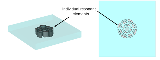
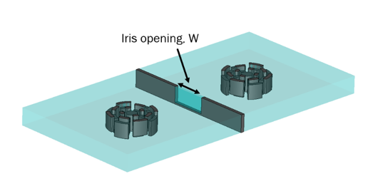
The actual inter-resonator coupling, as from (1), is equal to k12 = k23 = 0.02016. Effectively, the actual coefficient infers how much energy is coupled from one resonator to another. It is usually calculated using a system of two resonators, such as the one shown in Fig. 3. The resonator structure shown in Fig. 3 has 2 distinct resonant frequencies, which depend on the level of resonator coupling. This was well-explained in [6], however, it will be briefly repeated here. With reference to Fig. 4 (a), let us assume that a resonator in isolation operates at a resonant frequency . The resonant frequency is obtained by setting the input admittance, to zero. In a similar way, the zeroes of the coupled resonator system of Fig. 4 (b) are obtained by setting its input admittance, , Yin to zero. With reference to this figure, Yt represents the the admittance transformer with the characteristic admittance of. By setting Yin to zero, two distinct resonant frequencies are obtained, f1 and f2:
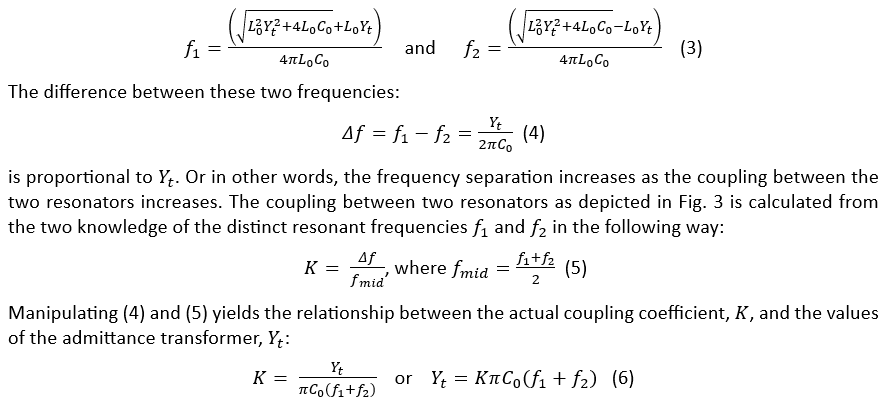
In this way, the relationship between the equivalent circuit of a filter (Fig. 1) and coupled resonators (Fig. 4 (b)), respectively, with coupling coefficients of (1) and (2) is established.
The resonant frequencies of the two-resonator structure of Fig. 3 can be obtained using an eigenmode solver of any commercially available full-wave resonator, such as Computer Studio, (CST) [7] or Ansys’ HFSS [8]. The coupling between the resonators in the present case is obtained using CST and is presented.
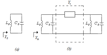
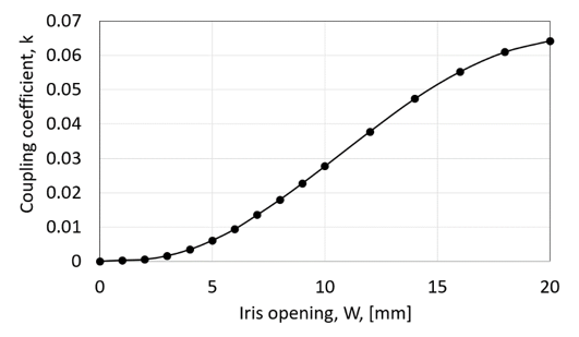
in Fig. 5 as a function of iris opening, W. Given the fact that inter-resonator coupling between two resonators, as inferred from the coupling matrix (1) is 0.02162, implies that the iris opening of, approximately, 8.2 mm should suffice, however, the exact value will be determined later, as elaborated in the section of filter tuning.
External coupling
The excitation of the input and output resonators provides the means for RF energy to enter and exit the filter. The level of excitation is primarily determined by the percentage bandwidth of the filter () and the values of the coupling coefficient/admittance transformer. In mathematical terms, the level of external coupling is given by:

Using filter specifications fo=1800 MHz, BW=40 MHz and M01=0.9728 or K01=0.02162, Qext is determined to be 47.55. This is the value of external coupling that will need to be exhibited at a centre frequency of a filter, f0=1800 MHz).
A filter can be excited in many ways and addressing different ways of excitation is the subject for another topic. For the present design, the first/last resonator is excited using a grounded pin, as shown in Fig. 6. For the calculation of Qext it is not required to simulate the entire filter – only the input/output resonators should suffice. In cases when the input and output coupling coefficients are not the same, the procedure will need to be repeated both for the input Qext_in and output Qext_out. The resonator of Fig. 6 is excited using a grounded pin, whose proximity to the resonator dictates the correct excitation bandwidth.
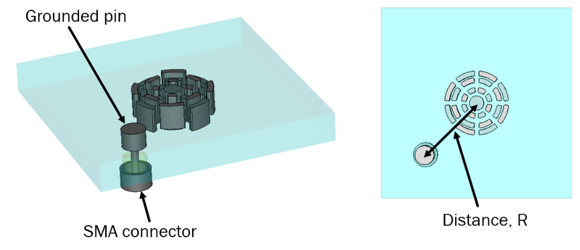

In general, the greater the distance between the feed pin and the resonator centre, the higher the loaded . Higher values of the result in lower excitation bandwidths.
The structure of Fig. 6 was simulated using a full-wave simulator, CST, for its reflection coefficient, . can be calculated from the reflection coefficient using the following equation:
Qext =fπ(delay (S_11 ))/2 (8)
The values of simulated for different separation values of R are plotted in Fig. 7.
For the present filter, the required value of external coupling is Qext =47.55 ,which, according to Fig. 7, is achieved by placing the feed pin at approximately R = 15.5 mm from the resonator centre. Having determined all the required coupling coefficients, we can now proceed to design the 3-pole filter.
Filter design and tuning
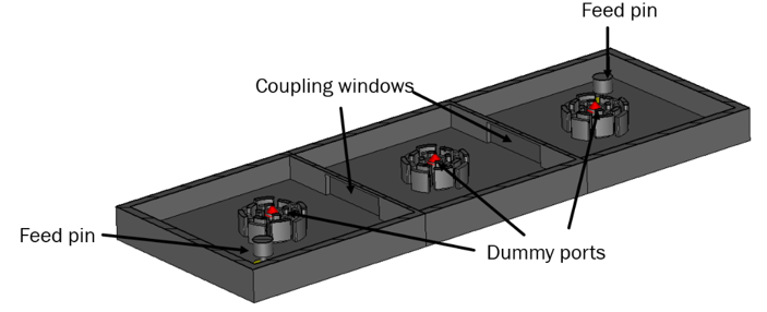
The designed filter is shown in Fig. 8. As per design requirements, the filter has 3 resonators and 2 coupling irises. The widths of the coupling irises is set to 8.2 mm, as inferred from Fig. 5 to obtain the coupling coefficient of 0.02016. In a similar way, the feed pins are positioned at a distance of R = 15.5 mm in order to obtain the loaded Qext =47.55 as required to correctly excite the filter. The filter is excited using 2 waveguide ports, positioned at the input/output. In addition to the waveguide ports, at the top of each resonator high impedance discrete ports are added. These ports play a major role in the tuning of the filter at a post-processing (tuning) step.
The initial simulated results of the filter as shown in Fig. 8 are shown in Fig. 9. As can be seen from Fig. 9, the initial response of the filter seems very close to the required characteristics, however, a closer.
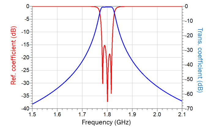
Inspection reveals that the reflection coefficient at the lower passband edge is higher than required -16 dB. This infers that the filter is not fully tuned, requiring fine tuning of both the resonant frequencies of the individual resonators and, also, the coupling coefficient. However, the question is which resonators and which coupling irises require tuning? This is impossible to predict by looking at the response of Fig. 9 alone. At this point, we introduce frequency domain tuning.
It was mentioned earlier in the text that dummy ports are introduced at the top of each resonator. These dummy ports will need to be assigned a high impedance in order not to interfere with the distribution of the Electro-Magnetic field inside the resonator.
Frequency domain tuning
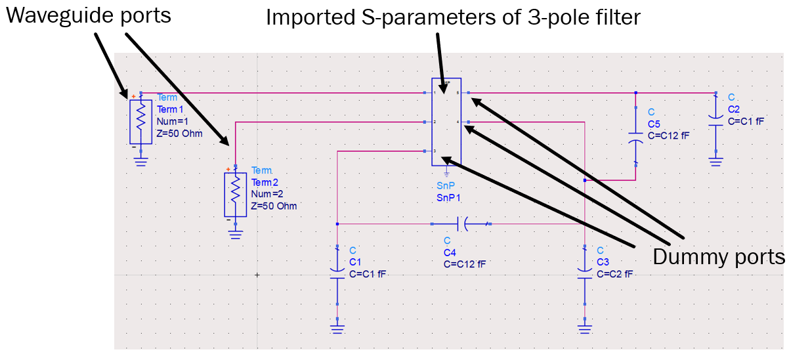
The first step towards frequency domain tuning lies with full-wave simulation of the filter of Fig. 8 with dummy ports attached, using commercially available software such as CST [7] or HFSS [8]. The port impedance of the dummy ports needs to be kept very high – in the present case, the port impedance is set to 100 GΩ. In the present case, the filter was simulated using CST. After the full wave simulation, the resultant s5p files are imported into a circuit simulator, as schematically depicted in Fig. 10. Waveguide (input/output) ports or ports 1 and 2 are terminated in 50 Ω impedance, whereas the dummy ports are terminated in ideal capacitors, C1, and C2. The C12 capacitor cross-connects capacitors C1, and C2. These capacitors are referred to as correction capacitors as their values are used to infer what type of correction (if any) needs to be applied to the physical filter of Fig. 8. Here, filter symmetry has been utilized to yield identical values for the correction capacitors attached to dummy ports 1 and 3 (C1). Correction capacitor C2 is attached to resonator 2. Correction capacitors C1 and C2 provide information with regards to the frequency or operation of the resonator to which they are attached. For example, if these capacitors are positive, this infers that the frequency of operation of the resonator needs to be reduced. Similarly, if their values are negative, the frequency of operation of the resonator needs to be increased. With regards to the cross capacitor, C12, its positive values infer that the coupling iris width needs to be reduced, while its negative values require the coupling iris to be widened. The coupling between resonators 1 and 2 and 2 and 3 is identical (as also seen from the coupling matrix (1) and (2)) and this is reflected in the identical value for the correction coupling capacitor, C12.
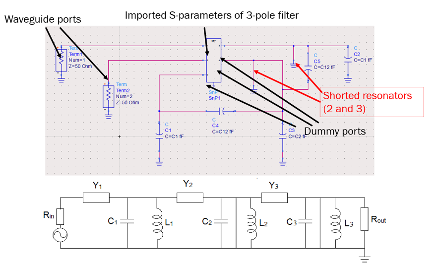
Frequency domain tuning is initiated by shorting all resonators expect the first resonator in the filter, Fig. 11 (top). Its circuit implementation is shown in Fig. 11 (bottom).
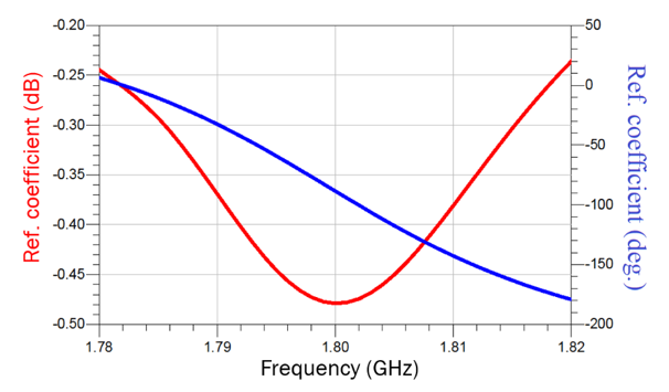
The response of the circuit of Fig. 11 is shown in Fig. 12. Since the dip of the reflection coefficient corresponds to 1.8 GHz, it can be inferred that the frequency of the first resonator (due to filter symmetry,
the third resonator also) is correctly tuned. We can now proceed to tune the second resonator. Before proceeding, we need to record the value of the phase of the reflection coefficient at the centre frequency of the filter. From Fig. 12, the phase of the reflection coefficient is equal to -88o. The tuning of the second resonator is initiated by removing the short circuit and adjusting the value of capacitor C2 until the phase of the reflection coefficient has been altered by + 180o. Given the fact that the phase of the reflection coefficient when the second resonator is shorted is – 88o, capacitor C2 is adjusted until the phase of the reflection coefficient becomes – 88o + 180o = 92o. This is achieved when the correction capacitor C2 attains the value of -3.6 fF. Removing the short circuit from resonator 3 (dummy capacitor value at this resonator
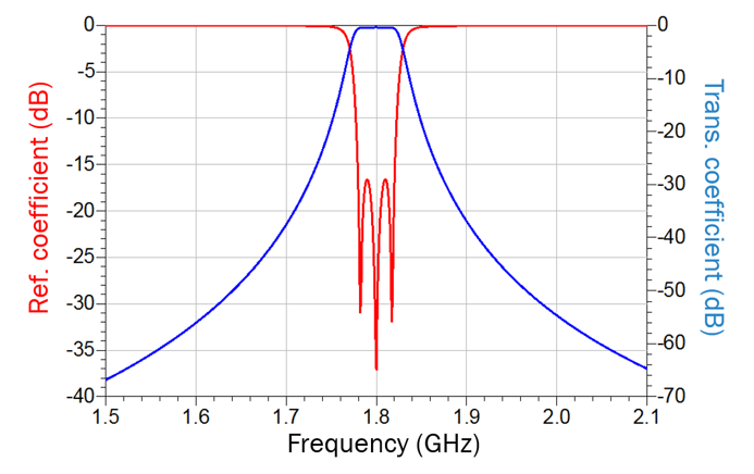
is identical to the dummy capacitor value on resonator 1) and leaving C12 = 0, the filter response using a circuit simulator of Fig. 13 is obtained. As can be seen, the response is much improved as the return loss now stands below -16 dB across the entire passband. However, a closer inspection reveals that a more symmetrical response is possible. Using the starting point with C1 = 0 fF, C2=-3.6 fF and C12 = 0 fF, the return loss was optimized using correction capacitors as independent parameters. The optimized filter response is shown in Fig. 14 and yielded the following values for the correction capacitors: C1 = 0.18 fF, C2=-4.2 fF and C12 = -0.31 fF. As can be seen, the of this filter is excellent. By iteratively applying the modifications to the designed filter of Fig. 8 in accordance with the correction capacitor values, one arrives at the final, tuned filter design once the values of the correction capacitors become either zero or very low values. For C1….Cn capacitors, this is reached when the magnitude of their values is lower than 1 fF and for C12….Cn-,n when the magnitude of their values is lower than 0.5 fF. The response of the filter after several iterations to reduce the levels of correction capacitors vs the filter with no correction capacitors is shown in Fig. 15. The values of correction capacitors are C1 = 0.35 fF, C2=-0.91 fF and C12 = 0.23 fF. As can be seen, the two responses are almost identical. Even though in principle it is possible to continue tuning until the
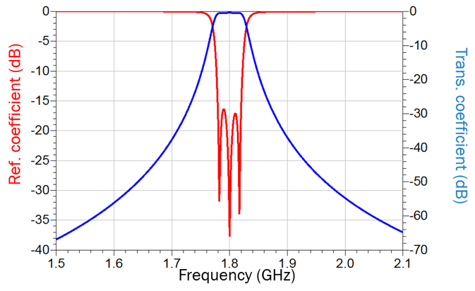
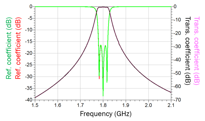
correction capacitors have reached even lower values, such a case is of limited use as it does not provide any additional insights. Furthermore, in practice tuning will almost always be performed using tuning and coupling screws, which have practical limits with regards to tuning accuracy.
In summary, frequency domain filter tuning consists of the following steps:
- Simulate a filter with waveguide and dummy ports attached. For planar filters one can use the Momentum engine in ADS and for 3D filters one can use full-wave simulators, such as CST [7] or HFSS [8].
- Export the obtained snp file into a circuit simulator
- Connect ideal capacitors to the dummy ports and standard RF ports to the input/output of the filter. Also, introduce “cross-connect” capacitors as in Figs. 10 and 11. The capacitors connected directly to the dummy ports control the frequency of operation of the resonator to which they are connected on and “cross-connect” capacitors control the extent of coupling. Set all capacitors to zero.
- Short all resonators apart from resonator 1 and run the circuit simulator. Using capacitor C1 tune the reflection coefficient until the dip in the reflection coefficient coincides with the centre frequency of the filter. Record the phase of the reflection coefficient at this frequency point.
- Remove the short circuit from resonator 2 and tune capacitor C2 until the phase of the reflection coefficient changes by +180o.
- Repeat steps 4 and 5 until the last resonator is reached. Once the last resonator is reached, remove its short circuit, and tune the last capacitor, Cn, until the maximum transmission coefficient is obtained. This concludes the tuning of the directly connected capacitors, C1….Cn and forms the starting point for the next step.
- Using the optimization feature in the circuit simulator optimize the response of the filter using the capacitors C1….Cn and C12….Cn-,n. Optimisation can be carried out with regards to the reflection or transmission coefficients and, sometimes, depending on the filter requirements, both.
- Upon completion of the optimization, use the values of the capacitors to influence the main filter design, i.e. change its physical characteristics – such as increase or reduce frequency of operation or coupling. If correction capacitors C1….Cn are greater than zero, reduce the frequency of operation of the concerned resonators. Alternatively, increase the frequency of operation. In a similar manner, if capacitors C12….Cn-,n are positive reduce the extent of coupling (usually by decreasing the size of the irises). Alternatively, increase the size of the irises.
- Repeat steps 7 and 8 until the correction capacitors become zero or attain very low values. Usually, the criterion is satisfied when the absolute values of C1….Cn are smaller than 1 fF and when the absolute values of C12….Cn-,n are smaller than 0.5 fF.
Conclusion
In this article a comprehensive study on how to design and tune an RF filter is presented. The study was initiated using basic filter principles applied to a practical filter design (three-pole filter). However, the principles outlined can be equally well applied to almost any filter design.
References:
[3] Handbook of filter synthesis, A. Zverev, ISBN 978-0-471-74942-4.
[5] S. Bulja, E. Doumanis and D. Kozlov, “Concentric distributed resonators and filters”, IEEE Radio and Wireless Symposium, Anaheim, California, US, 2018, pp. 267-269.
[6] S. Bulja and M. Gimersky, “Low profile distributed cavity resonators and filters,” in IEEE Trans. Microwave Theory and Tech., vol. 65, issue 10, pp.3769-3779, 2017.
[7] https://www.3ds.com/products/simulia/cst-studio-suite
[8] https://www.ansys.com/products/electronics/ansys-hfss
Leave a Reply