Microstrip antennas trace their history back to the 1950s, when the concept of microstrip radiator was introduced by Deschamps [1]. The development of the microstrip patch antenna, however, lay dormant until the early 1970, when their use became more widespread, primarily due to the improved availability of good substrates, with low-loss tangents and better theoretical models capable of better prediction of their performance. The very first practical microstrip antennas have been demonstrated by Howell [2] and Munson [3]. Since then, microstrip antennas have been the subject of intensive research and development, due to their attractive features, such as their low cost, low weight, low and conformable profiles and compatibility with integrated circuits.
However, practical microstrip antenna design still draws attention both from academia and industry, where the main focus is aimed at impedance bandwidth increase and desirable radiation characteristics (polarization, cross-polarization ratios, to name but a couple). Even though the design of such antennas has been greatly aided by the advent of full-wave simulation software packages, such as Computer Studio, CST [4] and HFSS [5], practical patch antenna design is still a matter of interest and is, particularly for the case of stacked patches, done, primarily, using trial and error. The particular problem relates to input coupling, coupling among stacked patches and their relative position with respect to each other in order to yield a broad impedance bandwidth and desirable radiation characteristics. In essence the problem relates to how a stacked antenna can be tuned. The literature is sparse on how this should be done in a systematic and repeatable fashion.
In this article we approach antenna design and tuning methodically using a combination of full-wave simulations, circuit simulations and filter theory. Such an approach allows us to tune the antenna for the broadest bandwidth possible using the frequency domain techniques in a prompt and straightforward fashion.
General principle
Despite their superficial differences, a great deal of work on filter theory can be readily applied to microstrip antenna design. For example, filters are composed of individual resonators which in the antenna case corresponds to individual patches. Further, just like in filter design, input coupling determines the extent of achievable bandwidth. What is different, though, is that the number of stacked patch antennas is usually smaller than the number of resonators in a filter. Stacked patch antennas usually have a maximum of three patches, whereas filter orders up to 10 are not unheard of. In a way, this makes stacked patch antennas easier to tune, but it needs to be understood that unlike in filters where the input and output impedances are usually, but not necessarily, 50 Ω, in antennas only the input is terminated in 50 Ω, whereas the output impedance of the antenna is given by Z0=Rout=√((μ0 μr)/(ε0 εr )), which in the case of air becomes Z0=Rout= √(μ0/ε0) ≈377 Ω. . This infers that if one were to utilize filter theory to design stacked antennas, such an analysis would only be valid in the first order approximation and optimization procedures will need to be used to address the impedance differential.
The general principle of stacked patch antenna tuning, as pursued in this article, using the frequency domain technique will be explained with reference to an ideal bandpass filter with no cross coupling, as depicted in Fig. 1. This follows up on our previous article, entitled, “How to design and tune an RF filter”, which provided steps with regards how filters can be tuned. With reference to this figure, the equivalent
circuit of a stacked patch antenna having a number of patches equal to n is represented using n resonators, with each resonator representing a patch in the antenna stack. The coupling among the patches and input

and output is represented using n+1 coupling (admittance transformation) sections. The resonators/patches in Fig. 1 are depicted using the parallel connection of capacitors (C1, C2, …Cn) and inductors (L1, L2,….Ln) and the coupling sections with admittance transformers Y1, Y2,…Yn.
Just like in the case with filters, the correct input and inter-resonator coupling coefficients can be calculated using either filter tables [6] or software packages such as Guided Wave Technology’s Filter & Coupling Matrix Synthesis Software [7]. The coupling coefficient at the input is calculated in a similar way. However, as mentioned earlier, the coupling coefficient values obtained in this way as applied to antennas would be only valid as the first order approximation, due to the existence of an impedance mismatch at the output. The best way to learn how to design and tune an antenna in the frequency domain is via an example.
Example – stacked 2-patch antenna
Let us design a microstrip antenna with 2 stacked patches, operating at a centre frequency of 11.72 GHz. The antenna is to be designed with a view of obtaining as wide bandwidth as possible, with a minimum return loss of 10 dB.
Solution: Since the bandwidth of the antenna is not specifically stated, the first step in the design relates to examining the maximum bandwidth the antenna can support. As we have learnt from the previous article on filter tuning, excitation (external coupling) plays an important role in determining the extent of the bandwidth the antenna can support.
External coupling
Antenna excitation provides the means for RF energy to enter the device. The level of excitation is primarily determined by the percentage bandwidth (BW/f0) and the values of the coupling coefficient/admittance transformer, as evident from Fig. 1. In mathematical terms, the level of external coupling is given by:

However, apart from the frequency of operation, f0=11.72 GHz , we have no knowledge of other parameters that would help us determine the right level of external coupling. This means that we will need to examine the maximum bandwidth that the antenna can provide. This is done through the parametric investigation of Qext of the first antenna patch. Just like with the case with filters, it is not necessary to simulate the entire stacked 2-patch antenna – the first patch is all that is required to infer the values of the Qext.
To this end, let us assume that the antenna is to be fed using a probe, as shown in Fig. 2, however, its exact position is to be determined with a view of maximizing the bandwidth. In addition, let us also assume that
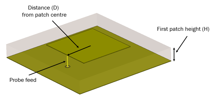
the substrate thickness of the probe-fed patch antenna is also a parameter, which we will use to determine the optimum height to support wide bandwidth.
The structure of Fig. 2 was simulated using a full-wave simulator, CST, for its reflection coefficient, S11. Qext . was then calculated from the reflection coefficient using an equation alternative to that of (1):

The patch of Fig. 2 has the dimensions of Xpatch = Ypatch = 6.63 mm and is mounted on Rogers RO3003 [8] substrate, with εr = 3 and tan(δ) = 0.001. The values of Qext simulated for different feed offset distances, D, and substrate thicknesses, H, are shown in Fig. 3. For the cases depicted in Fig. 3 (left), the distance from the probe feed to the patch centre is kept at D = 3 mm and, for the cases shown in Fig. 3 (right), the substrate height was kept at H = 0.75 mm.
For broad bandwidths, the values of Qext need to be as low as possible, as can be inferred from (1). From Fig. 3, it follows that the lowest values of Qext are recorded when the feed probe is positioned at the edge of the patch (Fig. 3 right) and when the substrate thickness is approximately 0.75 mm (Fig. 3 left). It is further obvious from Fig. 3 (left) that Qext is not a monotonous function of substrate thickness and that a range of substrate thicknesses exists for which the input impedance bandwidth is at a maximum; in the present case this corresponds substrate heights in the region from 0.5 mm – 1 mm. This point requires further elaboration.
Choosing the lowest substrate height is beneficial for several reasons. First, the impedance bandwidth of

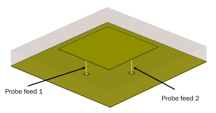
the antenna is maximized, while retaining a low profile. Second, lower substrate heights offer improved radiation characteristics as the cut-off frequency of surface waves is inversely proportional to substrate height. Thirdly, when used in configurations requiring dual or circular polarization, utilizing two probe feed structures as shown in Fig. 4, probe-fed patch antennas tend to suffer from a high cross-polarization ratio, compared to, for example, aperture fed patch antennas. This is primarily attributed to the fact that parasitic coupling exists between the two probe feeds. This is greatly reduced by reducing the profile of the antenna. This topic will be, however, covered in depth in another article.
For the broadest possible bandwidths, according to Fig. 3, the probe feed needs to be placed at 3 mm away from the patch centre and substrate thickness of 0.75 mm needs to be chosen. In this set-up, Qext becomes 6.657. Using CMS software [7] in conjunction with (1), the required frequency of operation of 11.72 GHz and Qext = 6.657, one obtains the coupling matrix for the double patch antenna:

Inter-resonator (patch) coupling
The actual inter-resonator (patch) coupling, as implied from (3), is equal to k12 = 0.2002016. Effectively, the actual coefficient infers how much energy is coupled from one patch to another. In standard filter settings it is determined using a system of two resonators in conjunction with an Eigenmode solver, which can calculate the natural frequencies of such a system. In the present case actual coupling between patches is calculated to a first order approximation using the two-patch structure shown in Fig. 5. In a manner similar to inter-resonator coupling with filters, the coupling between the two patches is obtained by monitoring the difference between the two resonant frequencies of the system of Fig. 5 as a function of displacement along the Y-axis:

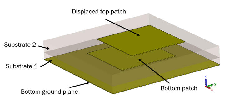
However, unlike in the calculations of the inter-resonator coupling in filter design where the Eigenmode solver can be used to infer the frequencies of the two-resonator system, here this is not possible. The primary reason for this lies with the fact that the Eigenmode solver is only applicable to closed form (bounded) structures, without the need for external excitation. In the case of antennas examined here, this is performed using a Time domain solver. To perform this task adequately, the antennas need to be very weakly excited, effectively mimicking the operation using the Eigenmode solver, with high Qext to avoid unnecessarily loading the antenna. This is accomplished by setting the positions of the probe-feed near to the centre of the bottom patch. In the present case, the probe-feed is located at a displacement distance of 1 mm from the centre of the patch. The sizes of both the bottom and top patches are kept the same – 6.63 mm in both the X and Y directions and the substrate thickness for the top patch is 1.25 mm. A typical response of the two-antenna system is shown in Fig. 6 (left). The coupling coefficients as a function of top patch displacement are shown in Fig. 6 (right) and are calculated using (5). The coupling among the patches is fully magnetic. From the coupling matrix (3), the necessary actual coupling coefficient of 0.20036 is obtained when the top patch is displaced with respect to the bottom patch by approximately 1.3 mm. This, in conjunction with the exact feed position obtained in the previous section enables us to proceed towards the design of the broadband antenna. This is elaborated in the next section.

Antenna design and tuning
The designed antenna is shown in Fig. 7. As per design requirements, the antenna consists of 2 stacked patches. The antenna is also fed using a probe, positioned 3 mm away from the centre of the bottom patch. The height of the bottom patch is 0.75 mm, and the height of the top patch is 1.25 mm. The top patch is displaced 1.3 mm relative to the bottom patch since, according to Fig. 6 (right), this gives rise to
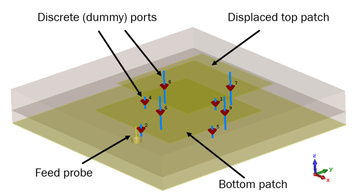
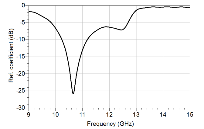
the required coupling coefficient of 0.20036. In order to allow antenna tuning in a post-processing step, discrete ports are added to each patch. It should be noted that unlike the case with filters, where each resonator has one discrete port attached, each antenna patch in this case has 4 discrete ports attached. This is needed to adequately ground the patch which will be required during the post-processing step. The reflection coefficient of the antenna as designed in Fig. 7 is shown in Fig. 8. As can be seen, the antenna is not fully tuned for wide bandwidth (-10 dB) as required by the specifications. This situation is similar to that of filter tuning addressed in our previous article, where the initial response needs refinement in order to fully satisfy requirements. In essence, the sizes of the patches and their relative displacement need to be tuned in order to yield an optimum response. This is performed using frequency domain tuning.
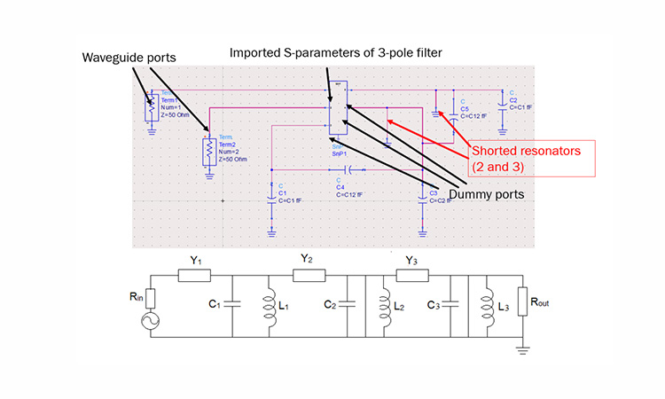
The first step towards antenna tuning lies with full-wave simulation of the filter of Fig. 7 with dummy ports attached, using commercially available software such as CST [4] or HFSS [5]. The port impedance of the dummy ports is, just like in the case of filter tuning, kept very high – in the present case, the port impedance is set to 100 GΩ. After the full wave simulation, the resultant s9p files are imported into a circuit simulator, such as Keysight’s Advanced Design System, (ADS), [9], as schematically depicted in Fig.9
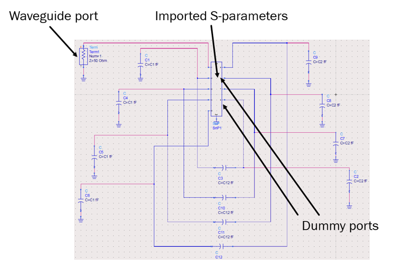
The waveguide port or port 1 is terminated in 50 Ω impedance, whereas the dummy ports are terminated in sets of ideal capacitors, C1, and C2. The C12 capacitor set cross-connects sets of capacitors C1, and C2 connected through dummy ports to the same sides of the antenna patches. These capacitors are referred to as correction capacitors as their values infer what type of correction (if any) needs to be applied to the physical antenna of Fig. 7. A set of identical correction capacitors, termed C1 are attached to the bottom patch, and, similarly, another set of identical capacitors, C2, are attached top the top patch. These capacitors are connected to each other using cross-capacitors, C12. Just like in the case with filter tuning, frequency correction capacitors C1 and C2 provide information with regards to the frequency or operation of the patch to which they are attached. For example, if these capacitors are positive, this infers that the frequency of operation of the patch needs to be reduced. Similarly, if their values are negative, the frequency of operation of the patch needs to be increased. With regards to the cross capacitor, C12, its positive values infer that the coupling between the two patches needs to be increased and as evident from Fig. 6 (right), this infers that the relative displacement between the patches needs to be increased. Similarly, negative values of C12 dictate that the displacement between the patches needs to be reduced.
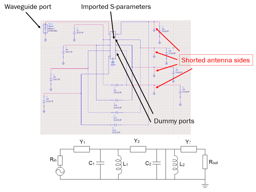
Frequency domain tuning is initiated by shorting all patches expect the first (bottom), as shown in Fig. 10 (top). Its circuit implementation is shown in Fig. 10 (bottom). Capacitor C1 is tuned until the dip of the reflection coefficient corresponds to the centre frequency of operation of the antenna – 11.72 GHz in this case. This is achieved then C1 = 28 fF. The response of the circuit of Fig. 10 is shown in Fig. 11. Before proceeding, just like in the case of filter tuning, we need to record the value of the phase of the reflection coefficient at the centre frequency, 11.72 GHz of the antenna. From Fig. 11, the phase of the reflection coefficient at 11.72 GHz is equal to -114o. Any subsequent patches, with the exception of the last patch, are tuned in an identical way as it was done with filters, i.e. by removing the short circuit of the next patch and tuning the phase of the reflection coefficient until it is altered by +180o. Since in the present case, the antenna consists of 2 patches and the second (top patch) is last, the procedure consists of varying the value of capacitor C2 in a circuit simulator until the optimal reflection coefficient has been achieved over the broadest bandwidth. In the present case this is achieved when C2 = -56 fF, with the corresponding
response shown in Fig. 12. As can be seen, the response is much improved compared to the return loss in Fig. 8. However, a closer inspection reveals that the -10 dB bandwidth is moved towards lower frequencies: from 10.47 GHz to 12.67 GHz. This infers that further optimization is likely to yield better results. Using
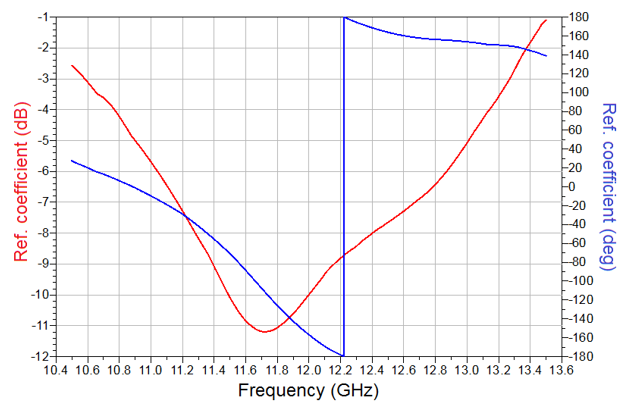
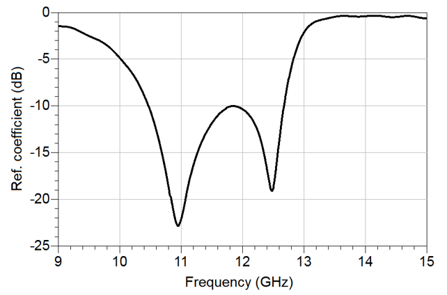
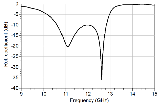
the starting point with C1 = 28 fF, C2=-35 fF and C12 = 0 fF, the return loss was optimized for broadest possible bandwidth (10.6 GHz-12.82 GHz) using correction capacitors as independent parameters. The optimized antenna response is shown in Fig. 13 and yields the following values for the correction capacitors: C1 = 25 fF, C2=-56 fF and C12 = -6.53 fF. As seen, the response of this antenna is excellent, however, the level of the correction capacitors needs to be reduced. By iteratively applying modifications to the designed antenna of Fig. 7 in accordance with the correction capacitor values, one arrives at the Final tuned antenna design once the values of the correction capacitors become either zero or attain very low values. The exact tolerable low values of these capacitors are dependent on the antenna’s impedance bandwidth, however, it is accepted that for C1….Cn capacitors this is usually reached when the magnitude
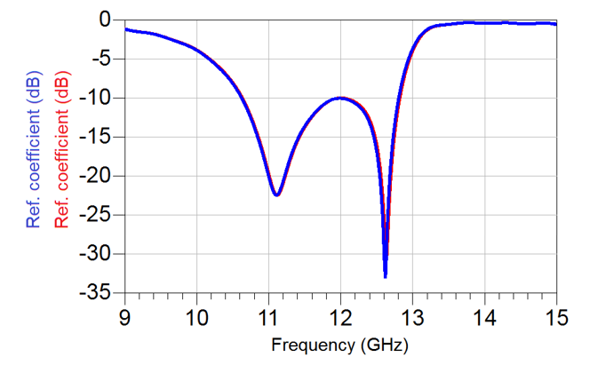
of their values is lower than 5 fF and for C12….Cn-,n when the magnitude of their values is lower than 2 fF. The response of the antenna after several iterations to reduce the levels of correction capacitors against the antenna with no correction capacitors is shown in Fig. 14. The values of correction capacitors are C1 = -1.39 fF, C2=-0.39 fF and C12 = -0.53 fF and the exact dimensions of the bottom and top patches are: Xbottom = Ybottom = 6.56 mm, Xto = Ytop = 6.08 mm, with a relative patch displacement of Ydisp = 1.02 mm. As can be seen, the two responses are almost identical. Even though in principle it is possible to continue antenna tuning until the correction capacitors have reached even lower values, such a case is of limited use as it does not provide any additional benefits. The antenna exhibits the -10 dB impedance bandwidth from 10.63 GHz to 12.82 GHz (BW = 2.19 GHz), which is slightly lower (0.1%) than the theoretically predicted impedance bandwidth of 2.21 GHz in (4).
In summary, the design and tuning of a wideband microstrip patch antenna consists of the following steps:
- Decide on the type of excitation to be used and fix its position to yield the lowest Qext. This part is dependent on the dielectric characteristics and height of the substrate. Refer to section “External coupling” for details.
- Decide on the number of patches – usually going beyond 3 stacked patches is impractical and designs using 2 stacked patches are most common.
- Using filter theory [6,7] and the values of Qext found in 1., calculate the coupling coefficients required for broad bandwidth and the desired number of antenna patches. Refer to section “External coupling” for details.
- Using the structure of Fig. 5 in conjunction with the time domain solver, infer first order patch displacement necessary for realization coupling coefficients for broad bandwidth. Refer to section “Inter-resonator (patch) coupling” for details.
- Simulate the antenna with waveguide and dummy ports attached. For stacked patch antennas one can use either the Momentum engine in ADS [9] or full-wave simulators, such as CST [4] or HFSS [5]. Use at least 4 dummy ports for each patch, ensuring that at least one dummy port is connected to a side of the individual patch.
- Export the obtained snp file into a circuit simulator.
- Connect ideal capacitors to the dummy ports and standard RF port to the input of the antenna. Also, introduce “cross-connect” capacitors as in Figs. 9 and 10, ensuring that the “cross-connect capacitors” connect frequency tuning capacitors on the side of the respective patches. The capacitors connected directly to the dummy ports control the frequency of operation of the resonator to which they are connected on and “cross-connect” capacitors control the extent of coupling. Set all capacitors to zero.
- Short all patches apart from the bottom (fed) patch and run the circuit simulator. Using capacitor C1 tune the reflection coefficient until the dip in the reflection coefficient coincides with the required centre frequency of the antenna. Record the phase of the reflection coefficient at this frequency point.
- Remove the short circuit from patch 2 and tune capacitor C2 until the phase of the reflection coefficient changes by +180o.
- Repeat steps 8 and 9 until the top patch is reached. Once the top patch is reached, remove its short circuit, and tune the last capacitor, Cn, until the minimum reflection coefficient is obtained across the bandwidth of interest. This concludes the tuning of the directly connected capacitors, C1…. Cn and forms the starting point for the next step.
- Using the optimization feature in the circuit simulator optimize the response of the antenna using the capacitors C1…. Cn and C12…. Cn,n. Optimization needs be carried out with regards to the reflection coefficient.
- Upon completion of the optimization, use the values of the capacitors to influence the main antenna design, i.e. change its physical characteristics – such as increase or reduce frequency of operation or coupling. If correction capacitors C1…. Cn are greater than zero, reduce the frequency of operation of the concerned patches. Alternatively, increase the frequency of operation. In a similar manner, if capacitors C12…. Cn,n are positive, increase the extent of displacement between the respective patches. Alternatively, reduce the extent of displacement.
- Repeat steps 11 and 13 until the correction capacitors become zero or attain very low values. Usually, the criterion is satisfied when the absolute values of C1…. Cn are smaller than 5 fF and when the absolute values of C12…. Cn,n are smaller than 2 fF.
Conclusion
In this article a comprehensive study on how to design and tune stacked microstrip patch antennas is presented. The study shows how one can maximize the impedance bandwidth of a stacked patch antenna in a systematic way by borrowing the theory developed for the design and tuning of RF filters. The study is initiated using basic filter principles applied to a practical antenna design (stacked 2 patch antenna). However, the principles outlined can be equally well applied to almost any antenna design.
References:
[1] Deschamp, G. A., “Microstrip Microwave Antennas,” 3rd USAF Symposium on Antennas, 1953.
[2] Howell, J. Q., “Microstrip antennas,” IEEE AP-S Int. Symp. Digest, 1972, pp. 177-180.
[3] Munson, R. E., “Conformal Microstrip Antennas and Microstrip Phased Arrays,” IEEE Trans. On Antennas and Propagation, vol. AP-22, 1974, pp. 74-78.
[4] https://www.3ds.com/products/simulia/cst-studio-suite
[5] https://www.ansys.com/products/electronics/ansys-hfss
[6] Handbook of filter synthesis, A. Zverev, ISBN 978-0-471-74942-4.
[8] https://www.rogerscorp.com/advanced-electronics-solutions/ro3000-series-laminates/ro3003-laminates
Leave a Reply